
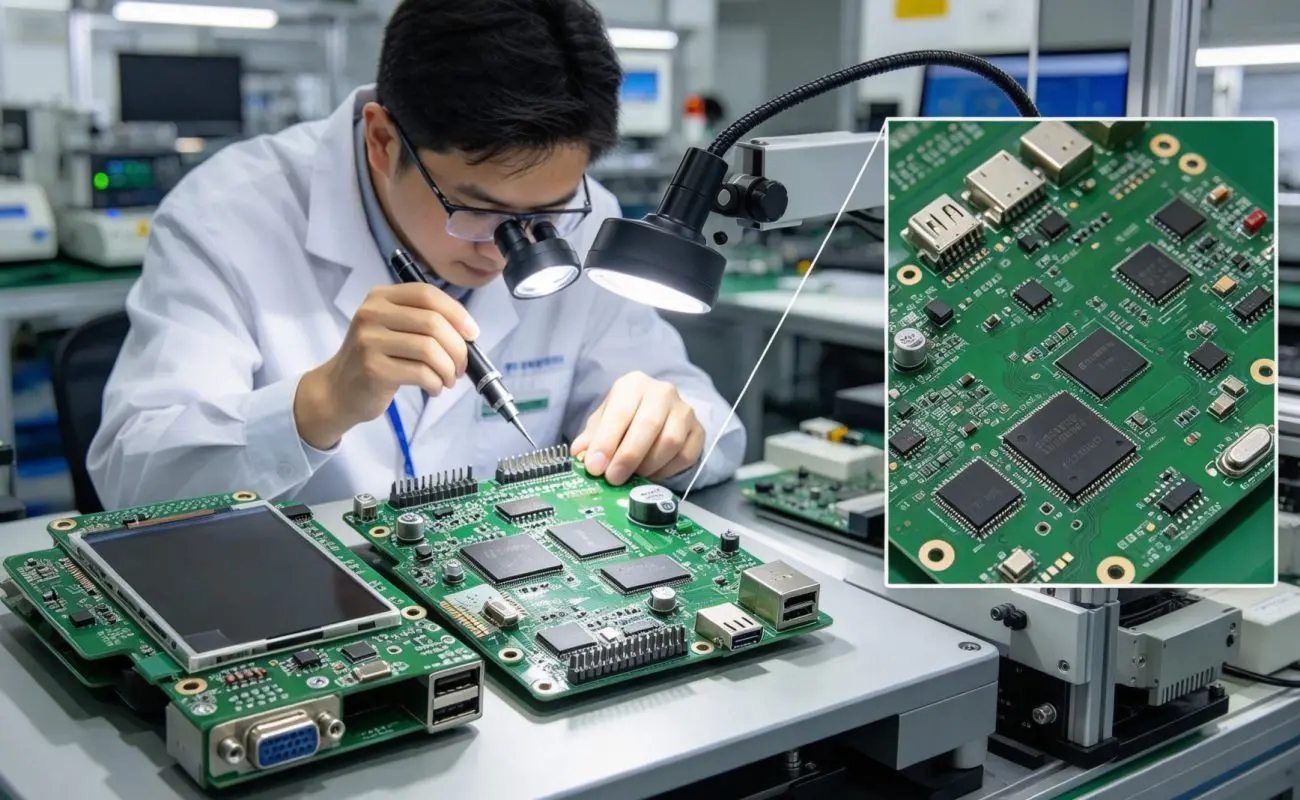
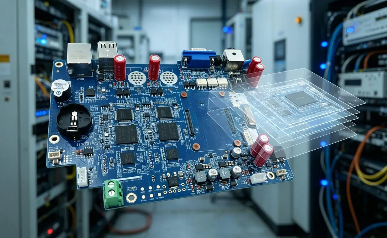
Industrial control electronics require circuit boards that balance electrical performance, manufacturing efficiency, and convenient maintenance. During PCB assembly and inspection, the solder mask is more than a protective coating because its color and surface quality can also affect how easily technicians identify potential defects. The 2-Layer FR4 industrial control PCBA uses a green LPI solder mask that provides a clear visual background for inspecting solder joints, component placement, and PCB surface conditions. As a result, the board supports both practical industrial control applications and efficient quality inspection workflows.
Why Green LPI Solder Mask Supports Visual Inspection
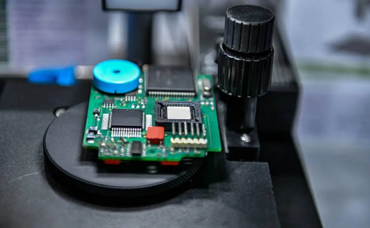
Green solder mask has long been widely used in PCB manufacturing because it creates clear contrast between the board surface, copper features, component bodies, and solder joints. During manual inspection, this contrast can help technicians identify missing components, solder bridging, exposed copper, or irregular solder coverage more easily. Moreover, the LPI process produces a controlled solder mask pattern around pads and traces, which helps maintain a clean and consistent board appearance. Therefore, green LPI solder mask can contribute to more convenient visual inspection throughout assembly and maintenance.
For industrial control PCBA production, several inspection benefits are particularly relevant:
- Clear surface contrast: Green solder mask makes component pads and solder joints easier to distinguish.
- Defect visibility: Surface abnormalities, exposed copper, and solder-related issues can be more noticeable.
- Inspection consistency: A uniform mask surface provides a stable visual background for repeated inspection.
- Maintenance convenience: Technicians can more easily identify visible changes during equipment servicing.
How the 2-Layer Structure Supports Industrial Control Designs
A two-layer PCB provides a practical balance between routing flexibility, board size, and manufacturing cost for many industrial control applications. In this design, the top and bottom copper layers can accommodate signal routing while copper pours provide ground and power areas. In addition, separated power domains such as 5V and 3.3V can help reduce unwanted interaction between analog and digital sections when the layout is properly designed.
The 2-Layer FR4 industrial control PCBA measures 100 × 79.69 mm with a 1.6 mm thickness, providing a compact platform for microcontrollers, communication interfaces, sensors, and power components. Furthermore, 1 oz copper supports practical power routing while the minimum 100 μm line and space capability allows relatively dense routing for low-speed interfaces such as UART and I2C. This combination makes the board suitable for compact control equipment where electrical organization and efficient use of PCB space are important.
FR4 Material and Industrial-Grade Construction
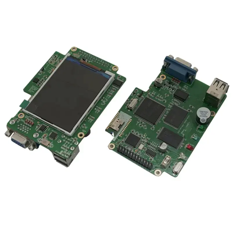
FR4 provides a useful combination of electrical insulation and mechanical rigidity for industrial electronic assemblies. With a dielectric constant of approximately 4.5, the material supports stable electrical performance in moderate-temperature environments. At the same time, the 1.6 mm board thickness provides sufficient mechanical support for both surface-mounted and through-hole components. The board also uses an ENIG surface finish, which helps protect exposed copper while providing a suitable surface for component soldering. Consequently, SMT and DIP components can be combined on the same board to accommodate different design requirements. This mixed assembly approach is especially useful when compact surface-mounted components need to work alongside robust connectors, terminal blocks, or relays.
Green LPI, ENIG, and SMT+DIP Assembly Working Together
Visual inspection is most effective when the PCB surface, component arrangement, and manufacturing quality work together. Green LPI solder mask provides the visual background, while ENIG offers a consistent finish on exposed contact areas. Meanwhile, combining SMT and DIP assembly allows designers to select appropriate component packages based on electrical, mechanical, and field-wiring requirements.
| Feature | Inspection or Manufacturing Benefit | Industrial Relevance |
|---|---|---|
| Green LPI solder mask | Clear visual contrast and surface protection | Easier assembly and maintenance checks |
| ENIG finish | Reliable solderable surface and corrosion protection | Supports long-term component assembly |
| SMT assembly | Supports compact component placement | Suitable for dense control circuits |
| DIP assembly | Provides robust through-hole connections | Useful for connectors and relays |
| 2-layer stackup | Balances routing and manufacturing requirements | Suitable for compact control equipment |
| FR4 substrate | Provides rigidity and electrical insulation | Supports industrial PCB construction |
Manufacturing Quality Control for Reliable Inspection
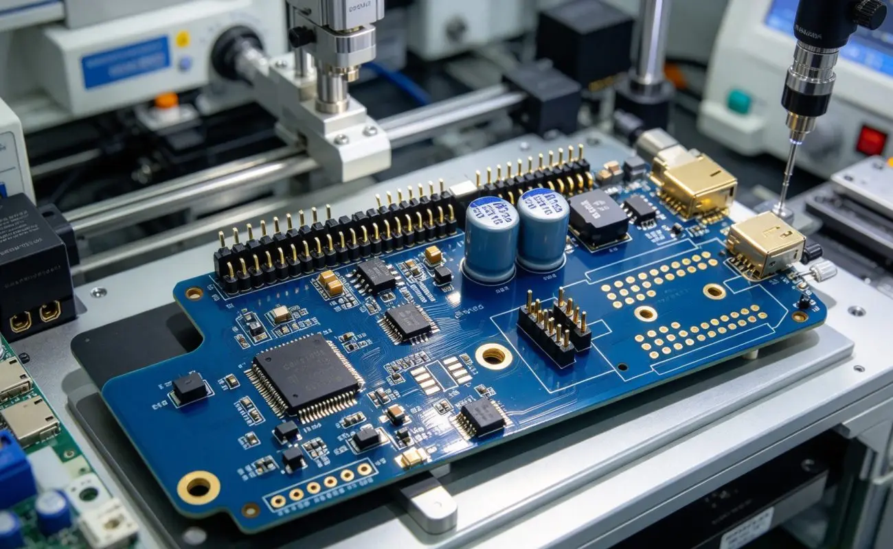
Visual inspection begins with consistent PCB fabrication, but automated testing provides an additional layer of quality control. Laser direct imaging can support accurate trace formation, while controlled copper plating helps maintain consistent conductivity across the board. After assembly, automated optical inspection can check component placement, solder mask coverage, and visible assembly conditions.
The manufacturing process also incorporates several inspection and testing steps:
- AOI inspection checks visible assembly conditions and potential component or solder defects.
- Flying probe testing verifies electrical continuity and isolation to identify open or short circuits.
- Thermal stress testing evaluates solder-joint reliability through controlled reflow cycles.
- Visual inspection provides an additional check of board appearance, soldering, and component placement.
As a result, combining fabrication controls with optical and electrical testing provides a more complete quality assessment than relying on visual inspection alone.
Applications in Industrial Control Equipment
The 2-Layer FR4 industrial control PCBA can support several types of industrial electronics where compact construction and reliable signal or power management are required. For example, sensor modules can combine temperature, humidity, or pressure sensing with signal conditioning and wireless communication. Similarly, motor control units can use PWM control, current limiting, and protection functions to manage low-voltage motors in equipment such as conveyors. Other applications include communication interface boards and power distribution circuits. A communication board can support protocol conversion such as RS-485 to USB, while a power distribution board can manage 24V DC loads with protective components and status indicators. Therefore, the same PCB architecture can be adapted to different industrial control functions depending on component selection and circuit design.
B2B PCBA Manufacturing for Industrial Projects
For industrial equipment manufacturers, sourcing a PCBA involves more than selecting a substrate and copper layer count. Consistent fabrication, assembly quality, inspection capability, and application requirements all influence the suitability of a board for production. Fully Hong can support industrial PCBA requirements involving PCB fabrication and assembly, helping customers develop boards suited to automation, sensing, communication, and power management applications.
Ultimately, the 2-Layer FR4 industrial control PCBA combines a practical two-layer architecture with FR4 construction, green LPI solder mask, ENIG finishing, and mixed SMT+DIP assembly. More importantly, the green solder mask provides a clear visual surface that can make inspection and maintenance more convenient. With controlled manufacturing and multiple testing stages, this type of PCBA can provide a practical foundation for compact industrial control equipment.




Leave a reply