
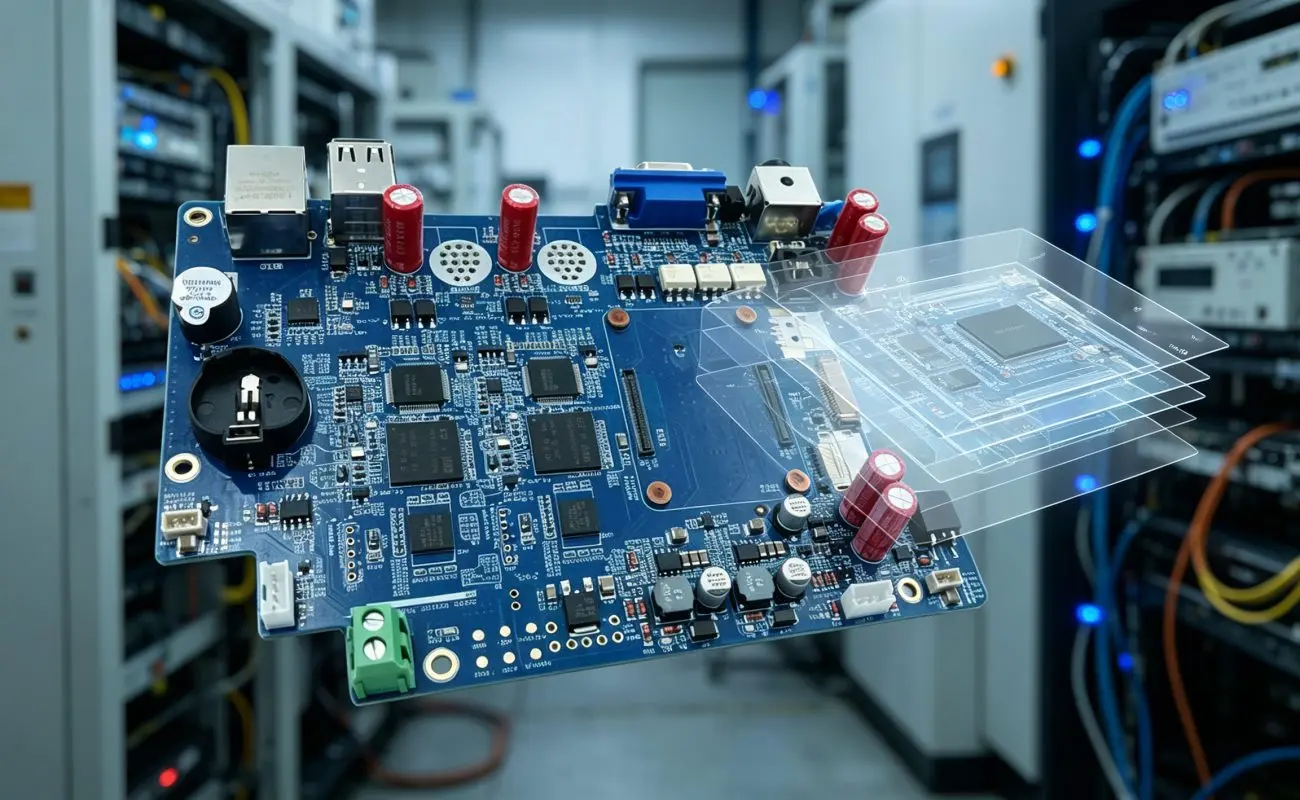
With the rapid development of industrial communication, automation equipment, and high-speed electronic systems, PCB designs need to provide more than simple electrical connections. Modern applications require stable signal transmission, reduced interference, and reliable operation under complex working conditions. Therefore, multilayer PCB structures with accurate impedance control have become essential for high-performance electronic devices.
The impedance controlled 8 layer PCB is specially designed to support high-speed signal transmission by optimizing layer structures, routing methods, and electrical performance. Through advanced microstrip and stripline configurations, this type of PCB helps reduce signal reflection and maintain signal integrity in industrial communication systems. Fully Hong provides professional PCB manufacturing solutions to meet the requirements of customers in automation, communication, and advanced electronic applications.
Why Microstrip and Stripline Structures Improve Signal Integrity
In high-speed PCB design, signal quality is strongly affected by transmission line structure. Microstrip and stripline configurations are two commonly used routing methods that help engineers achieve stable electrical performance. Microstrip structures place signal traces on the outer layer of the PCB with a reference plane underneath. This configuration provides easier manufacturing and convenient component routing, making it suitable for many high-speed interfaces. Meanwhile, stripline structures place signal traces between two reference planes inside the PCB stackup, offering better electromagnetic shielding and stronger noise control. Furthermore, selecting the appropriate routing structure helps maintain consistent impedance values and minimizes signal distortion. As a result, high-speed interfaces such as Ethernet, CAN communication, and differential signal channels can achieve more reliable data transmission.
Advanced 8-Layer Stackup Supports Complex Circuit Integration
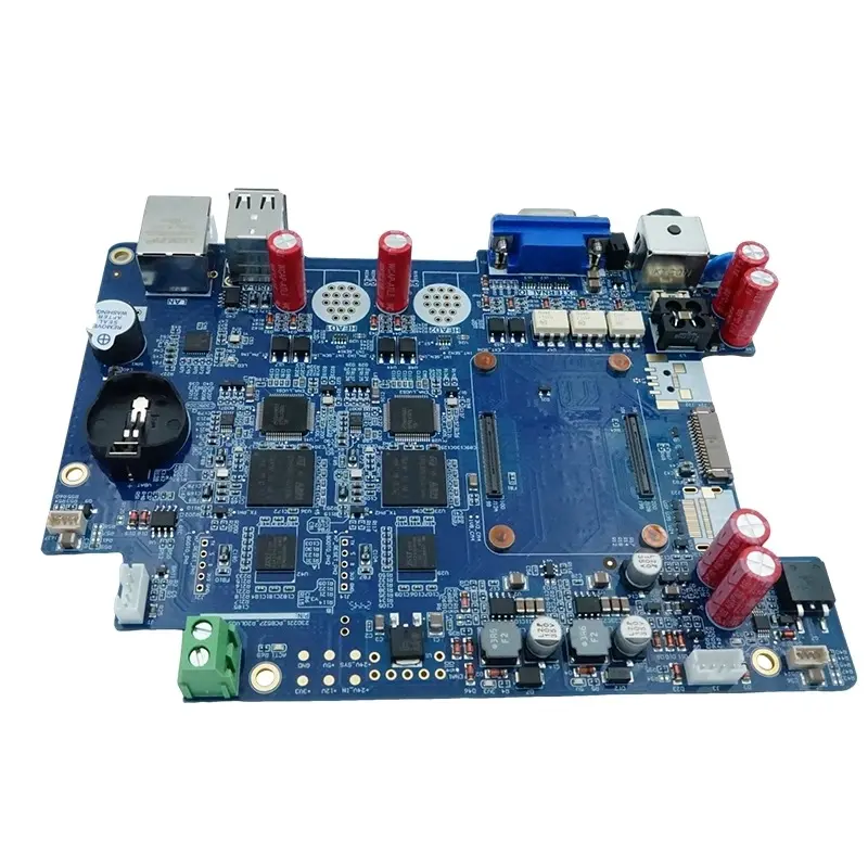
An 8-layer PCB provides more space for signal routing, power distribution, and grounding optimization compared with traditional two-layer or four-layer boards. The combination of multiple signal layers and power/ground planes creates a stable electrical environment for demanding applications. The impedance controlled 8 layer PCB features an optimized stackup design with four signal layers and four power/ground layers. This structure effectively reduces electromagnetic interference (EMI) while providing dedicated routing paths for high-speed differential signals. Additionally, the board size of 174.52×121.25mm and thickness of 1.6mm offer a balance between compact design and mechanical strength. Therefore, it can be integrated into industrial control cabinets, communication gateways, and automation equipment where space and reliability are both important.
Precision Impedance Control for High-Speed Applications
Maintaining accurate impedance is one of the most important factors in high-frequency PCB manufacturing. If impedance values change significantly, signal reflections and transmission errors may occur, affecting overall system performance. This PCB supports precise impedance control with differential impedance of 100Ω±8% and single-ended impedance of 50Ω±8%. These specifications help ensure stable signal transmission for high-speed communication interfaces. Moreover, the use of 1oz copper thickness supports fine-line routing while maintaining good current-carrying capability. With a minimum line and spacing design of 75μm/75μm, the PCB can achieve high-density circuit integration without compromising electrical reliability.
Industrial-Grade Manufacturing Ensures Long-Term Reliability
Beyond electrical performance, manufacturing quality also plays a critical role in PCB reliability. Industrial applications often involve vibration, temperature changes, and electromagnetic interference, so the PCB must maintain stable performance over long operating periods.
Fully Hong applies advanced manufacturing technologies, including Laser Direct Imaging (LDI), to achieve precise trace formation. Furthermore, ENIG surface treatment provides excellent corrosion resistance and long-term solderability, while the blue LPI solder mask helps protect circuits and improves visual identification during assembly and maintenance. The impedance controlled 8 layer PCB also supports mixed assembly processes, including SMT for high-density components such as PHY chips and FPGAs, as well as DIP assembly for durable connectors and relays.
Key Advantages of Impedance Controlled 8 Layer PCB
- Optimized Signal Routing: Supports microstrip and stripline configurations for high-speed transmission.
- Accurate Impedance Control: Maintains stable electrical performance with controlled impedance values.
- Strong EMI Suppression: Multi-layer stackup improves signal protection and reduces interference.
- High-Density Integration: Supports complex industrial communication circuit designs.
- Reliable Surface Treatment: ENIG finish improves durability and connection stability.
- Industrial Compatibility: Suitable for demanding automation and communication environments.
Comparison Between Microstrip and Stripline Configurations
| Comparison Factor | Microstrip Configuration | Stripline Configuration |
|---|---|---|
| Signal Layer Position | Located on external PCB layers | Located between internal reference planes |
| EMI Protection | Good shielding performance | Better electromagnetic isolation |
| Manufacturing Difficulty | Easier production process | Requires more precise layer control |
| Application Advantage | Suitable for accessible high-speed routing | Ideal for critical signal integrity applications |
| Typical Usage | Ethernet interfaces, general high-speed signals | High-frequency and sensitive communication circuits |
Reliable PCB Solution for Industrial Communication Systems
As electronic systems continue moving toward higher speeds and greater integration, PCB design must focus on both electrical performance and manufacturing reliability. A properly designed multilayer PCB can significantly improve communication stability and extend equipment service life. The impedance controlled 8 layer PCB provides a reliable foundation for industrial Ethernet networks, PLC systems, railway communication equipment, and wireless communication devices. By combining advanced stackup technology, precise impedance management, and durable manufacturing processes, it helps engineers achieve consistent performance in demanding applications.
With professional PCB manufacturing experience, Fully Hong continues to provide customized circuit board solutions that support modern electronic innovation. Through precise design and strict quality control, this PCB technology enables customers to build more reliable, efficient, high-performance systems.




Leave a reply