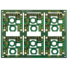
8-layer FR4 PCB is engineered for high-density electronic designs that require a balance of signal integrity, 配电, and compact form factors, such as consumer electronics, 医疗器械, and industrial control modules. 这 8-分层架构 (typically 4 信号层 + 4 电源/接地层) enables complex routing for fine-pitch components while minimizing electromagnetic interference (电磁干扰). 这 1.2毫米板厚 offers a lightweight yet rigid foundation, ideal for space-constrained applications where weight and durability are critical.
Constructed with FR4材质, the PCB provides reliable electrical insulation (介电常数εr=4.5) and mechanical stability, suitable for a wide range of operating environments. 这 2奥兹 (70微米) 铜厚 on all layers enhances current-carrying capacity (每条迹线高达 15A) while maintaining design flexibility for both power and signal traces. 这 Green LPI (液体光成像) 阻焊层 not only protects the circuitry from environmental damage but also improves visual inspection accuracy, 而 白色丝印 ensures clear component marking and designations for assembly and maintenance.
A key feature is the 同意 (化学镀镍沉金) surface treatment, which provides a smooth, corrosion-resistant finish for excellent solderability. The nickel layer (3–5μm) 增加耐用性, and the gold layer (0.05–0.1μm) prevents oxidation, making it suitable for long-term use. 这 POFV (Plated Over Filled Vias) technology further enhances the PCB’s reliability: vias are filled with conductive material and plated over, eliminating voids that could cause thermal stress or solder wicking. This is particularly important for high-density designs with fine-pitch components (例如, 0.5mm pitch BGAs) and ensures consistent performance in reflow soldering processes.
Manufacturing this PCB involves advanced techniques to ensure precision and quality:
- 激光直接成像 (LDI) achieves fine-line accuracy (最小线宽/间距: 50μm/50μm) for complex routing.
- POFV processing uses conductive epoxy or resin to fill vias, followed by plating to create a smooth surface.
- 100% 兴趣区 (自动光学检测) verifies solder mask coverage and silkscreen clarity.
- Electrical testing ensures continuity and isolation resistance, meeting IPC-6012 Class 2 standards.
Engineers will appreciate the PCB’s versatility in handling both high-density signal routing and moderate power applications. In consumer electronics, it supports compact designs for smartphones, 片剂, and wearables, where space is at a premium. In medical devices, the POFV technology and ENIG finish contribute to long-term reliability in diagnostic equipment. In industrial systems, the 2OZ copper and FR4 material provide the durability needed for control panels and automation modules.
By choosing this 8-layer FR4 PCB with 2OZ copper, ENIG finish, and POFV technology, customers gain a solution that balances density, 可靠性, 和成本效益. Its combination of advanced via filling, premium surface treatment, and precise manufacturing makes it a strategic choice for applications where component integration and long-term performance are essential. 由 ISO 支持 9001:2015 认证, this PCB ensures consistent quality from prototyping to mass production.

")