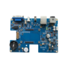
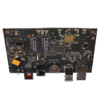
This power supply PCBA solution addresses the rigorous demands of high-power electronics, combining 6-layer signal/power separation with conformal coating for environmental protection. Các 1.60mm-thick 6-layer FR4 PCB (Tg ≥170°C) ensures thermal stability and low impedance in power delivery, while the multi-layer architecture separates high-voltage domains from low-level control signals to minimize EMI—critical for efficient power conversion. Các Lớp phủ phù hợp (typically polyurethane or acrylic) provides a waterproof, dustproof, and corrosion-resistant barrier, ideal for power supplies operating in harsh environments.
- In dán:
- In stencil chất hàn không chì (SAC305) with ±5% volume accuracy for power MOSFETs and fine-pitch ICs.
- SPI (Kiểm tra dán hàn):
- 3D optical verification of paste deposition to prevent solder bridging in high-current paths.
- Nhặt & Đặt các thành phần:
- Vị trí có độ chính xác cao (±30μm) của các thành phần SMT, bao gồm cả cuộn cảm điện, DC-DC converters, and 0.5mm pitch controllers.
- hàn lại:
- Dòng chảy lại được hỗ trợ bằng nitơ (đỉnh điểm 260°C) for void-free joints on ENIG surfaces, critical for heat dissipation in power devices.
- Aoi (Kiểm tra quang học tự động):
- Post-reflow inspection for solder defects, sai lệch thành phần, and polarity errors.
- Tht (Công nghệ xuyên lỗ):
- Chèn các đầu nối dòng điện cao, máy biến áp, and electrolytic capacitors via automatic inserters.
- Hàn sóng:
- Hàn sóng không chì (250-260°C) with nitrogen for reliable through-hole joints in power terminals.
- Hàn tay:
- Precision manual soldering for heat-sensitive components or custom heat sink installations.
- Lớp phủ phù hợp:
- Uniform application of conformal coating (thickness: 25-50μm) via spray or dip process, with curing at 60-80°C.
- Kiểm tra FG (Kiểm tra chức năng):
- Load testing under full/half/no load conditions, voltage regulation, efficiency measurement, and overcurrent protection verification.
- Kiểm tra chất lượng:
- Final audit including coating coverage check, Hi-Pot test (1000Trong DC), and insulation resistance measurement (≥100MΩ).
- SPI: Ensures solder paste consistency in power device pads to prevent thermal runaway.
- Kiểm tra bằng tia X: Verifies BGA/CSP joint integrity in controller ICs, đảm bảo <5% voiding.
- Kiểm tra chức năng: Simulates overload, short circuit, and input voltage fluctuations (±10%) for reliability.
- Conformal Coating QC: Optical microscopy to check coating uniformity and coverage on all components.
- Hi-Pot Test: Verifies isolation between high-voltage (HV) and low-voltage (LV) domains to prevent arcing.
- Chế tạo PCB:
- 6-layer FR4 with 1.60mm thickness, 2OZ copper on power layers, 1OZ on signal layers, and thermal via arrays for heat dissipation.
- Gia công linh kiện:
- Sourcing of power-grade components (ví dụ., Infineon MOSFETs, TDK inductors, Teapo high-temperature capacitors).
- SMT&Tích hợp THT:
- Mixed technology assembly supporting power modules (ví dụ., Igbts, SiC MOSFETs) và IC điều khiển.
- Kiểm tra & Chứng nhận:
- Tuân thủ IEC 62368 (an toàn điện), TRONG 61000 (EMC), và UL 60950 cho thiết bị công nghệ thông tin.
- Nguồn điện công nghiệp:
24V/48V DC power supplies for factory automation, with active PFC and remote monitoring.
- Máy chủ & PSU trung tâm dữ liệu:
Hiệu quả cao (≥90%) power supplies for 1U/2U servers, supporting 80 PLUS Platinum certification.
- Biến tần năng lượng tái tạo:
Bộ biến tần DC-AC cho hệ thống năng lượng mặt trời/gió, featuring MPPT control and grid-tie functionality.
- Trạm sạc EV:
High-power DC chargers (60kW-150kW) with galvanic isolation and thermal management.