
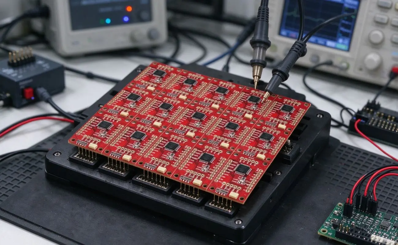
Wearable devices continue to become smaller, lighter, and more functional. Products such as fitness trackers, wireless modules, hearables, and portable medical sensors must integrate multiple electronic components into limited internal spaces. Therefore, PCB design and assembly play an important role in balancing compact dimensions, electrical performance, and manufacturing reliability. A small-size 2-layer FR4 PCBA board provides a practical solution for applications that require efficient component placement without the complexity of multilayer structures. However, maximizing space efficiency requires careful consideration of board dimensions, copper design, component selection, and SMT assembly processes.
Why Is a 2-Layer FR4 PCBA Suitable for Wearable Devices?
Wearable electronics often operate under strict size and weight limitations. Unlike larger industrial equipment, these devices have limited internal space for circuit boards, batteries, sensors, and wireless communication components. A two-layer structure provides conductive routing on both sides of the board, allowing engineers to distribute connections more efficiently. Consequently, it can support compact electronic designs while maintaining a relatively straightforward manufacturing process.
FR4 is widely used because it offers electrical insulation, mechanical stability, and cost-effective fabrication. For this particular design, the board measures 40mm × 25mm with a thickness of 1.6mm, making it suitable for compact electronic assemblies. Furthermore, the 1OZ (35μm) copper thickness on both layers supports signal routing and current distribution for battery-powered applications. A small-size 2-layer FR4 PCBA board can therefore help engineers balance circuit functionality, manufacturing cost, and limited installation space.
How Can PCB Layout Improve Space Efficiency?
An efficient PCB layout is essential when multiple components must fit within a small footprint. Engineers need to consider component dimensions, connection distances, trace routing, and mechanical clearance before finalizing the design. In addition, placing components according to their electrical functions can reduce unnecessary routing complexity and improve assembly efficiency. This makes layout planning an important part of custom PCB development.
Several design practices can help maximize available board space:
- Optimize component placement: Position frequently connected components close to each other to reduce routing distance and unnecessary trace crossings.
- Use compact component packages: Select suitable small-footprint components, such as 01005, 0201, and 0402 passive devices, according to assembly capabilities.
- Utilize both board surfaces: Place suitable components on both sides when mechanical clearance and assembly requirements allow.
- Reduce unnecessary routing: Plan signal paths carefully to avoid excessive trace length and improve layout organization.
- Maintain electrical clearance: Ensure adequate spacing between conductive features to support insulation and manufacturing requirements.
Moreover, engineers should evaluate component height as well as the horizontal board footprint. For wearable products with limited enclosure depth, the supplied design supports component heights up to 5mm. Therefore, coordinating PCB dimensions with the product enclosure early in development can help prevent mechanical interference during final assembly.
How Do FR4 Material and ENIG Finish Support Reliable Connections?
Material selection directly influences PCB durability and electrical performance. FR4 provides a stable substrate for electronic components while maintaining the insulation needed between conductive layers. Meanwhile, 1OZ copper on both sides supports signal transmission and power distribution for compact circuits. However, actual current capacity depends on trace width, temperature rise, operating conditions, and the surrounding thermal environment.
Surface treatment is another important consideration, especially when working with fine-pitch components. ENIG (Electroless Nickel Immersion Gold) creates a smooth, corrosion-resistant surface that supports reliable soldering. The supplied design uses a nickel layer of 3–5μm and a gold layer of 0.05–0.1μm, making it suitable for fine-pitch component assembly down to 0.3mm pitch. In addition, the red LPI solder mask protects exposed circuitry, while white silkscreen provides clear component identification for inspection and maintenance.
| PCB Feature | Specification | Design Benefit |
|---|---|---|
| Layer Count | 2 layers | Supports compact circuit routing |
| Board Dimensions | 40mm × 25mm | Fits space-constrained devices |
| Board Thickness | 1.6mm | Provides mechanical support |
| Base Material | FR4 | Electrical insulation and stability |
| Copper Thickness | 1OZ (35μm) | Supports signal and power routing |
| Surface Finish | ENIG | Corrosion resistance and solderability |
| Solder Mask | Red LPI | Circuit protection and visual identification |
| Silkscreen | White | Clear component markings |
These features work together to provide a practical foundation for compact electronic assemblies. Nevertheless, engineers should select specifications according to the actual electrical, mechanical, and environmental requirements of the finished product.
Why Is SMT Assembly Important for Miniature PCB Designs?
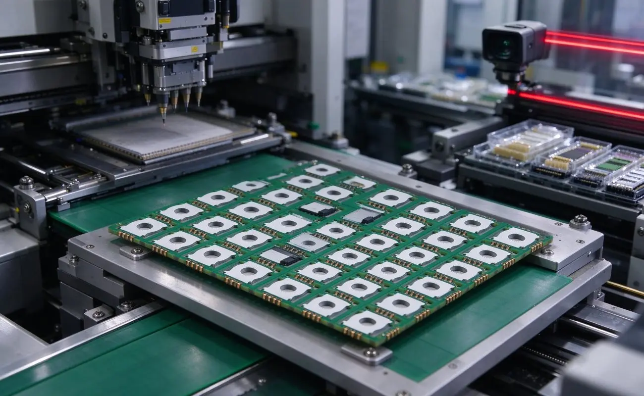
SMT Assembly allows electronic components to be mounted directly onto PCB surfaces, making it particularly useful for small electronic products. Compared with conventional through-hole assembly, SMT supports higher component density and automated placement. As a result, manufacturers can integrate more functions into limited board areas while maintaining consistent production processes.
The supplied PCBA design supports a range of component packages, including 01005 to 1206 passive components, QFP, BGA with 0.5mm pitch, and other miniature packages. Lead-free reflow soldering with a peak temperature of 260°C is used for component attachment. Furthermore, automated optical inspection (AOI) helps examine solder joint quality, while X-ray inspection can be used for BGA and CSP packages.
A complete printed circuit board assembly process may also include additional testing options:
- In-Circuit Testing (ICT): Checks electrical connections and component functionality.
- Functional Testing (FT): Evaluates whether the assembled board performs according to customer specifications.
- AOI Inspection: Identifies visible soldering and component placement issues.
- X-ray Inspection: Examines hidden solder joints in BGA and CSP packages.
By combining precision placement with appropriate inspection methods, manufacturers can improve assembly consistency and identify potential defects before shipment.
How Does a 4×5 Panel Format Improve Production Efficiency?
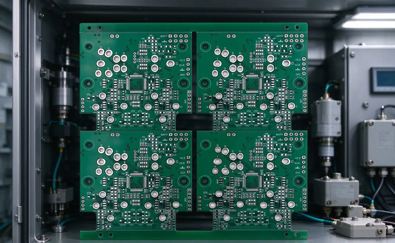
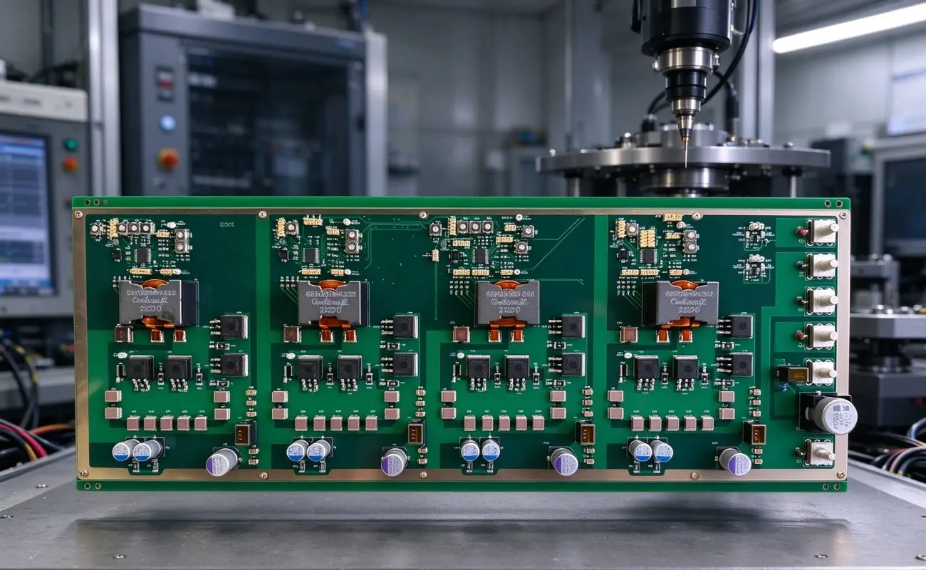
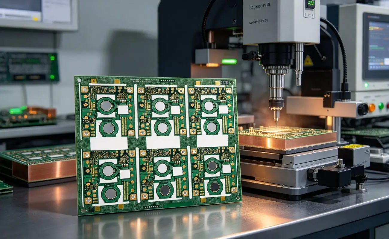
Panelization is another useful strategy for manufacturing small PCB assemblies. Instead of processing individual boards separately, multiple identical units can be arranged within a larger production panel. The supplied 4×5 panel format accommodates 20 identical boards, helping improve material utilization and streamline handling during assembly. Additionally, breakaway tabs and V-cut scoring support convenient depaneling after production.
This arrangement offers several manufacturing advantages:
- Higher production efficiency: Multiple boards can pass through assembly equipment within one panel.
- Reduced handling requirements: Panelized boards are easier to transport and process during automated SMT operations.
- Cost optimization: Shared setup and processing operations can improve production economics for larger quantities.
- Equipment compatibility: The format supports standard pick-and-place equipment, including Yamaha and Juki machines.
For high-volume projects, panelization can also help improve consistency across production batches. However, the final panel arrangement should consider board spacing, tooling requirements, depaneling methods, and component placement near board edges.
What Quality Standards Should Buyers Consider?
Quality control is essential when sourcing assembled PCBs for wearable and medical electronic applications. Even a compact board with well-planned routing may experience reliability problems if material traceability, soldering quality, or electrical testing is insufficient. Therefore, buyers should evaluate both manufacturing capabilities and inspection procedures before selecting a supplier.
The supplied design includes RoHS-compliant component requirements, a UL 94V-0 FR4 material rating, and IPC-A-610 Class 2 assembly quality criteria. It also specifies thermal cycling from -40°C to +85°C for 100 cycles and humidity testing at 85°C/85% RH for 1,000 hours. These requirements provide reference points for evaluating material properties and environmental reliability. In addition, ISO 9001:2015 quality management supports consistent manufacturing and process control.
At Fully Hong, PCB assembly requirements can be evaluated according to board dimensions, component specifications, surface finish, and production quantities. By coordinating PCB fabrication and assembly requirements, customers can develop compact electronic products with more consistent manufacturing specifications.
Conclusion
Maximizing space efficiency in wearable devices requires a combination of compact PCB dimensions, thoughtful component placement, reliable materials, and precise assembly processes. A two-layer FR4 design offers a practical balance between circuit functionality and manufacturing simplicity. Meanwhile, ENIG surface treatment, miniature SMT components, automated inspection, and panelized production help support consistent assembly quality. By integrating these considerations into the development process, a small-size 2-layer FR4 PCBA board can provide a suitable foundation for wearable electronics, wireless modules, and compact medical sensors.

Leave a reply