
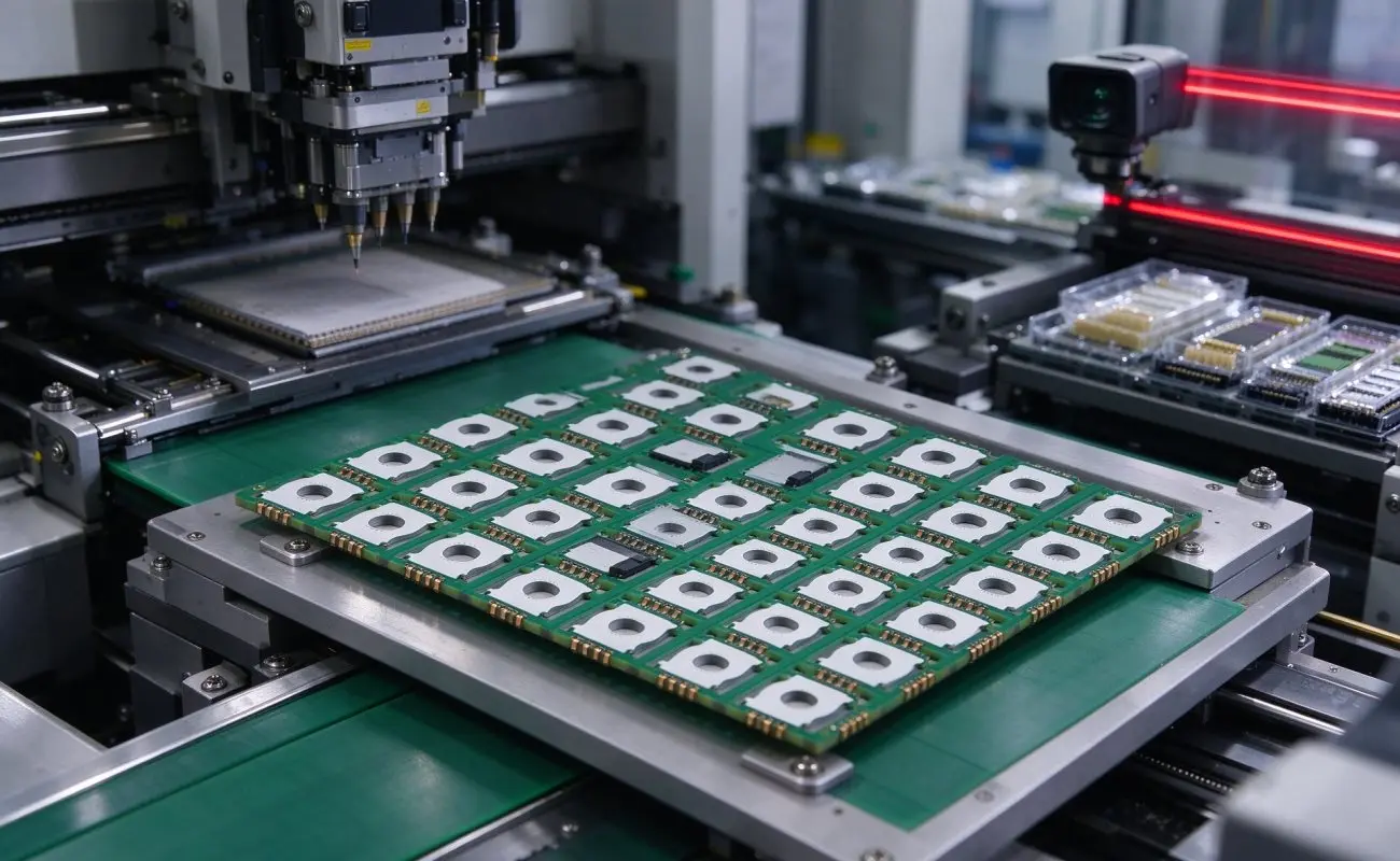
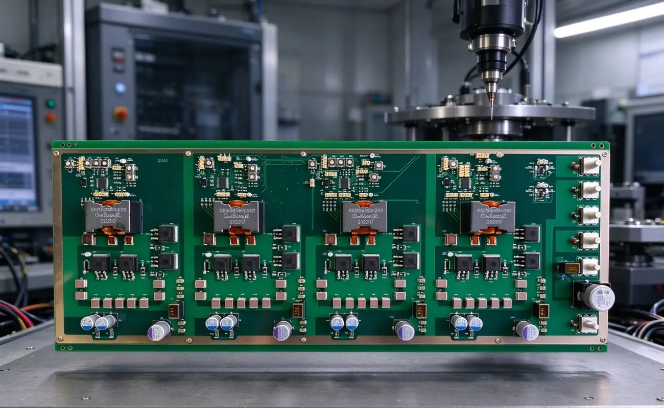
Medical devices increasingly integrate advanced electronic components into smaller and more compact structures. From diagnostic equipment to patient monitoring systems, these applications require stable signal transmission, reliable power distribution, and consistent electrical performance. A high-density 8-layer FR4 PCB provides multiple routing and grounding layers, allowing engineers to manage complex circuits within limited board space. However, achieving reliable signal integrity requires more than simply increasing the number of PCB layers. Stack-up design, impedance control, copper thickness, via structures, and surface treatment must work together to support stable operation.
Why Is an 8-Layer PCB Suitable for Complex Medical Devices?
Medical electronics often combine processors, sensors, communication interfaces, and power management circuits on a single board. As a result, conventional two-layer or four-layer designs may not provide enough routing space or sufficient separation between sensitive signals and power circuits. An 8-layer architecture creates additional signal and reference planes, allowing engineers to organize different circuit functions more effectively. Consequently, it becomes easier to manage electromagnetic interference (EMI) and reduce unwanted coupling between adjacent signal paths.
A typical 8-layer stack-up can include four signal layers and four power or ground planes, although the final arrangement should depend on the electrical requirements of the design. Ground planes provide continuous reference paths for high-speed signals, while dedicated power planes help distribute voltage across different circuit sections. Moreover, carefully arranged dielectric layers help engineers control impedance and minimize signal reflections. This makes multilayer PCB technology particularly useful for compact medical electronics that require multiple high-speed interfaces.
How Does Stack-Up Design Improve Signal Integrity?
Stack-up planning is one of the most important stages in high-density PCB development. When signal traces are placed too close to noisy power circuits or lack a suitable reference plane, electromagnetic interference and crosstalk may increase. Therefore, engineers should establish a clear layer arrangement before beginning detailed routing. A high-density 8-layer FR4 PCB can provide more flexibility for separating sensitive analog signals, high-speed digital interfaces, and power distribution networks.
Several design practices can help improve signal integrity:
- Maintain continuous reference planes: Place high-speed signal layers next to solid ground planes to provide stable return paths.
- Separate sensitive circuits: Keep low-level analog signals away from switching power circuits and other potential noise sources.
- Control trace impedance: Adjust trace width, copper thickness, and dielectric spacing according to interface requirements.
- Reduce unnecessary vias: Minimize layer transitions where practical to reduce parasitic inductance and discontinuities.
- Manage differential pairs: Maintain consistent spacing and routing geometry to support balanced signal transmission.
In addition, engineers should evaluate the complete current return path rather than focusing only on signal trace length. Proper reference-plane design helps reduce loop area and unwanted radiation. Consequently, a well-planned stack-up supports more predictable electrical performance during actual device operation.
How Do FR4 Material and Copper Thickness Affect PCB Performance?
FR4 is widely used in multilayer PCB manufacturing because it offers a practical balance of electrical insulation, mechanical stability, and manufacturing cost. Its dielectric properties influence signal propagation and impedance calculations, while its mechanical strength supports compact electronic assemblies. For the supplied 8-layer design, the dielectric constant is approximately 4.5, and the board thickness is 1.2 mm. These specifications provide a lightweight yet rigid structure for space-constrained medical and industrial applications.
Copper thickness is equally important, especially when signal routing and power distribution share limited board space. The supplied design uses 2OZ (70 μm) copper on all layers, providing increased current-carrying capacity compared with thinner copper constructions. This makes the board suitable for moderate-power circuits while supporting complex signal routing. However, actual current capacity depends on trace width, temperature rise, copper distribution, and operating conditions, so engineers should verify the design through appropriate calculations.
| PCB Feature | Supplied Specification | Engineering Benefit |
|---|---|---|
| Layer Count | 8 layers | Supports complex circuit routing |
| Base Material | FR4 | Electrical insulation and mechanical stability |
| Board Thickness | 1.2 mm | Compact and lightweight construction |
| Copper Thickness | 2OZ (70 μm) | Supports higher current capacity |
| Dielectric Constant | εr = 4.5 | Supports impedance design calculations |
| Surface Finish | ENIG | Provides corrosion resistance and solderability |
| Via Technology | POFV | Supports fine-pitch component assembly |
| Minimum Line/Space | 50 μm / 50 μm | Enables high-density routing |
These specifications should be considered together rather than evaluated independently. For example, thicker copper can improve current handling, but it may also affect fine-line fabrication requirements. Therefore, balancing copper thickness, trace geometry, and dielectric structure is essential for reliable PCB development.
Why Are ENIG Finish and POFV Technology Important?
Surface treatment and via construction can significantly influence the reliability of high-density electronic assemblies. ENIG PCB finish uses an electroless nickel layer followed by a thin immersion gold layer to provide a smooth, corrosion-resistant surface. In the supplied design, the nickel thickness is 3–5 μm, while the gold thickness is 0.05–0.1 μm. This combination supports consistent solderability and helps protect exposed copper from oxidation during storage and assembly.
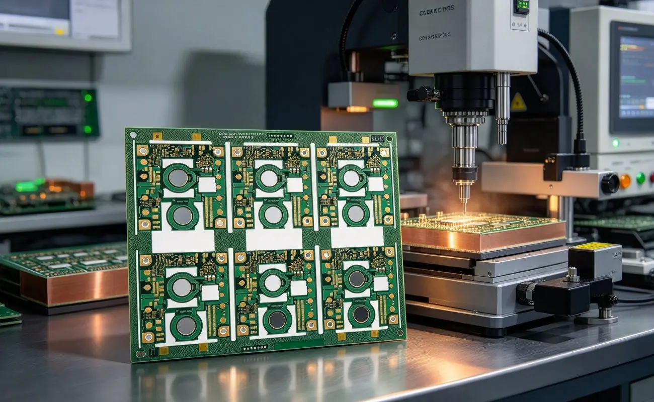
POFV, or Plated Over Filled Vias, is another important manufacturing process for compact PCB layouts. It involves filling vias with conductive material or resin and then plating over the filled structures to create a smooth surface. As a result, it helps reduce surface irregularities and supports component mounting over filled vias. This is particularly valuable for fine-pitch components such as 0.5 mm pitch BGAs, where via placement and surface flatness can influence assembly quality.
Together, ENIG and POFV provide practical advantages for multilayer designs with dense component arrangements. Nevertheless, process control remains essential because via filling quality, plating uniformity, and surface preparation can affect long-term reliability.
What Manufacturing Processes Help Ensure PCB Quality?
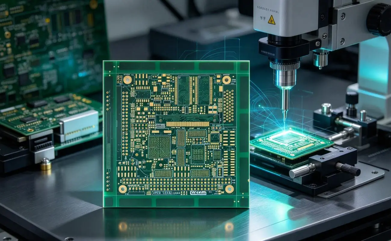
Reliable PCB performance depends on precision throughout fabrication and inspection. Even a carefully designed circuit can experience problems if fine-line patterns, plated vias, or solder mask coverage do not meet the required specifications. Therefore, manufacturers need suitable production equipment and quality control procedures to maintain consistency.
Key manufacturing and inspection processes include:
- Laser Direct Imaging (LDI): Helps achieve accurate fine-line patterns with a minimum line width and spacing of 50 μm/50 μm.
- POFV processing: Fills and plates vias to create a smoother surface for dense component layouts.
- Automated Optical Inspection (AOI): Checks circuit patterns, solder mask coverage, and silkscreen quality.
- Electrical testing: Verifies circuit continuity and isolation resistance to identify potential electrical defects.
- Process quality management: Supports consistent production according to applicable specifications, including IPC-6012 Class 2 requirements.
Furthermore, inspection should be integrated into different manufacturing stages rather than limited to the final production step. This approach helps identify potential issues earlier and supports more consistent results from prototypes to mass production.
Where Are High-Density FR4 PCBs Commonly Used?
High-density FR4 designs are suitable for applications that require compact circuit integration and dependable electrical connections. In medical electronics, they can support diagnostic equipment, monitoring devices, and other systems that combine sensors, processors, and communication modules. Meanwhile, consumer electronics benefit from their ability to accommodate multiple components within limited space.
Industrial PCB applications also require stable power distribution and reliable signal transmission. For example, automation controllers, control panels, and industrial monitoring modules may combine digital processing with moderate-power circuits. A high-density 8-layer FR4 PCB with 2OZ copper, ENIG finish, and POFV technology can address these integration requirements when the electrical and environmental specifications are properly matched.
At Fully Hong, PCB manufacturing considerations include material selection, layer configuration, copper thickness, surface finishing, and production quality control. By evaluating these factors together, engineers and purchasing teams can identify suitable PCB solutions for different electronic applications.
Conclusion
Maintaining signal integrity in complex medical devices requires careful coordination between PCB stack-up design, material properties, routing strategies, and manufacturing processes. An 8-layer architecture provides additional routing flexibility, while FR4 material and 2OZ copper support electrical insulation and power distribution requirements. Furthermore, ENIG surface treatment and POFV technology help address solderability and fine-pitch assembly challenges. By combining appropriate engineering design with precise fabrication and inspection, manufacturers can produce reliable multilayer boards for medical, consumer, and industrial electronics.

Leave a reply