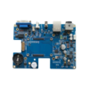
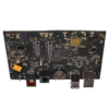
Diese PCBA-Lösung für die Stromversorgung erfüllt die hohen Anforderungen der Hochleistungselektronik, Kombination aus 6-lagiger Signal-/Leistungstrennung mit konformer Beschichtung zum Schutz der Umwelt. Der 1.60mm dicke 6-lagige FR4-Leiterplatte (Tg≥170°C) sorgt für thermische Stabilität und niedrige Impedanz bei der Leistungsabgabe, während die mehrschichtige Architektur Hochspannungsdomänen von Steuersignalen mit niedrigem Pegel trennt, um EMI zu minimieren – entscheidend für eine effiziente Leistungsumwandlung. Der konforme Beschichtung (typischerweise Polyurethan oder Acryl) sorgt für Wasserdichtigkeit, staubdicht, und korrosionsbeständige Barriere, Ideal für Netzteile, die in rauen Umgebungen betrieben werden.
- Drucken Einfügen:
- Schablonendruck von bleifreier Lotpaste (SAC305) mit ±5 % Volumengenauigkeit für Leistungs-MOSFETs und Fine-Pitch-ICs.
- Spi (Inspektion von Lotpasten):
- 3D Optische Überprüfung des Pastenauftrags zur Vermeidung von Lotbrücken in Hochstrompfaden.
- Wählen & Komponenten platzieren:
- Hochpräzise Platzierung (±30μm) von SMT-Komponenten, einschließlich Leistungsinduktivitäten, DC-DC-Konverter, und 0,5-mm-Pitch-Controller.
- Reflow-Löten:
- Stickstoffunterstütztes Reflow (Spitzentemperatur 260°C) für hohlraumfreie Fugen auf ENIG-Oberflächen, entscheidend für die Wärmeableitung in Leistungsgeräten.
- Aoi (Automatisierte optische Inspektion):
- Post-Reflow-Inspektion auf Lötfehler, Komponentenfehlausrichtung, und Polaritätsfehler.
- Tht (Durchloch-Technologie):
- Einsetzen von Hochstromsteckverbindern, Transformatoren, und Elektrolytkondensatoren über automatische Einleger.
- Wellenlöten:
- Bleifreies Wellenlöten (250-260° C) mit Stickstoff für zuverlässige Durchgangsverbindungen in Stromanschlüssen.
- Handlöten:
- Präzises manuelles Löten für wärmeempfindliche Komponenten oder kundenspezifische Kühlkörperinstallationen.
- Konforme Beschichtung:
- Gleichmäßiges Auftragen der Schutzbeschichtung (Dicke: 25-50μm) im Sprüh- oder Tauchverfahren, mit Aushärtung bei 60-80°C.
- FG-Test (Funktionstest):
- Belastungstest unter Voll-/Halb-/Leerlastbedingungen, Spannungsregelung, Effizienzmessung, und Überprüfung des Überstromschutzes.
- QS-Inspektion:
- Abschlussaudit inklusive Beschichtungsüberprüfung, Hi-Pot-Test (1000In DC), und Isolationswiderstandsmessung (≥100 mΩ).
- Spi: Stellt die Konsistenz der Lötpaste in den Pads von Leistungsgeräten sicher, um ein thermisches Durchgehen zu verhindern.
- Röntgeninspektion: Überprüft die Integrität der BGA/CSP-Verbindung in Controller-ICs, sicherzustellen <5% entleeren.
- Funktionstest: Simuliert Überlastung, Kurzschluss, und Eingangsspannungsschwankungen (±10 %) für Zuverlässigkeit.
- Qualitätskontrolle der konformen Beschichtung: Optische Mikroskopie zur Überprüfung der Beschichtungsgleichmäßigkeit und -abdeckung auf allen Bauteilen.
- Hi-Pot-Test: Überprüft die Isolierung zwischen Hochspannung (HV) und Niederspannung (LV) Domänen, um Lichtbögen zu verhindern.
- PCB-Herstellung:
- 6-Schicht FR4 mit 1,60 mm Dicke, 2Unzen Kupfer auf Leistungsschichten, 1OZ auf Signalschichten, und thermische Via-Arrays zur Wärmeableitung.
- Komponenten-Outsourcing:
- Beschaffung von Komponenten für die Stromversorgung (Z.B., Infineon MOSFETs, TDK-Induktoren, Teapo-Hochtemperaturkondensatoren).
- SMT&THT-Integration:
- Baugruppe mit gemischter Technologie zur Unterstützung von Leistungsmodulen (Z.B., IGBTs, SiC-MOSFETs) und Steuer-ICs.
- Testen & Zertifizierung:
- Übereinstimmung mit IEC 62368 (elektrische Sicherheit), IN 61000 (EMC), und UL 60950 für Geräte der Informationstechnik.
- Industrielle Stromversorgungen:
24V/48V DC-Netzteile für die Fabrikautomation, mit aktiver PFC und Fernüberwachung.
- Server & Netzteile für Rechenzentren:
Hocheffizient (≥90 %) Netzteile für 1U/2U-Server, unterstützend 80 PLUS Platin-Zertifizierung.
- Wechselrichter für erneuerbare Energien:
DC-AC-Wechselrichter für Solar-/Windanlagen, Mit MPPT-Steuerung und Netzkopplungsfunktion.
- Ladestationen für Elektrofahrzeuge:
Hochleistungs-DC-Ladegeräte (60kW-150 kW) mit galvanischer Trennung und Thermomanagement.