
PCB VIA (Vertical Interconnect Access)
VIA, short for Vertical Interconnect Access, is a crucial element in multi-layer printed circuit boards (多氯联苯). These copper-plated holes allow electrical and thermal connections between layers, supporting compact, high-performance electronic devices.
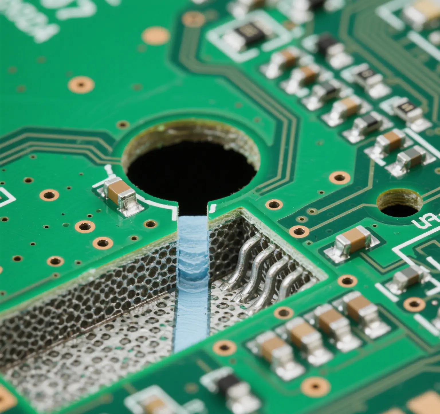
What Is a VIA?
一个 via is a small hole drilled (mechanically or by laser) through PCB layers, filled or plated with copper, enabling electrical continuity between layers. It consists of:
-
Barrel: The conductive tube lining the hole.
-
Pad: The copper ring that connects the via to a trace.
-
Anti-pad: The clearance around the via to isolate it from non-connected copper layers.
🔧 How Are Vias Made
-
Copper pads are placed on each layer.
-
Holes are drilled through the stack at connection points.
-
这 epoxy resin is removed chemically, exposing copper pads.
-
The barrel is formed by electroplating copper inside the hole.
-
阻焊层 is applied to protect and isolate.
✔️ This process allows engineers to stack multiple layers efficiently, minimizing board size while maximizing circuit complexity.
🔍 Types of Vias
1️⃣ Through-Hole Vias
Fully penetrates the PCB from top to bottom.
优点:
-
Strong mechanical and electrical connection
-
Good thermal conductivity
-
Easy for inspection and rework
-
Supports through-hole components
局限性:
-
Consumes space on all layers
-
Larger drill sizes limit layout density
-
May introduce signal reflections at high frequencies
Use Cases: Power/ground connections, connector mounting, thermal transfer.
2️⃣ Blind Vias
Connects outer layer to one or more inner layers, but doesn’t go through the entire board.
Benefits:
-
Increases routing density
-
Shorter electrical paths = better high-frequency performance
-
Saves board space
-
Reduces total layer count in complex designs
应用领域:
Mobile devices, high-speed circuits, 可穿戴电子产品, aerospace systems.

3️⃣ Buried Vias
Completely enclosed inside the board—connects inner layers only, invisible from the outside.
Manufacturing Challenges:
-
Requires sequential lamination and drilling
-
Needs precise alignment
-
Harder to inspect (requires X-ray)
优点:
-
出色的信号完整性
-
Lower EMI emissions
-
Frees up surface area
-
Greater routing flexibility
应用领域: High-speed designs, RF boards, compact multilayer PCBs
Choosing the Right Via
| Via Type | Layer Connection | 成本 | Space Saving | Signal Integrity |
|---|---|---|---|---|
| Through-hole | Full stack | 低的 | ❌ | Medium |
| Blind | Outer to inner | Medium | ✅ | High |
| Buried | Inner to inner only | High | ✅✅ | Very High |
| Micro via | Laser-drilled, small size | Very High | ✅✅✅ | Excellent |
Why Vias Matter in Modern PCBs
Vias support:
📡 Signal routing across layers
🔌 Power distribution and grounding
🌡️ Thermal management
🧩 High-density interconnects (HDI)
🎯 Precision performance in compact electronics
概括
Vias are core elements in multi-layer PCB design. They impact everything from performance and size to manufacturing cost and signal integrity. Selecting the right via type is crucial for your product’s success in today’s fast-evolving electronics landscape.