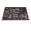
This 4-layer FR4 TG170 PCB is a high-reliability electronic substrate designed to meet the stringent requirements of the automotive industry, backed by IATF16949 certification. Engineered for applications ranging from advanced driver-assistance systems (ADAS) to in-vehicle infotainment and powertrain control, the PCB combines thermal stability, Tính toàn vẹn tín hiệu, and mechanical robustness to thrive in the harsh automotive environment.
Constructed from FR4 material with a glass transition temperature (Tg) ở nhiệt độ 170°C, this PCB outperforms standard FR4 (Tg130°C) in high-temperature scenarios, such as under-the-hood installations or prolonged operation in extreme climates. The 1.6mm thickness provides optimal mechanical rigidity to withstand vehicle vibrations (5-500Hz) and shocks, while the 1OZ (35μm) copper on all layers ensures reliable current handling (up to 8A per trace) and efficient heat dissipation via thermal vias. This makes it ideal for automotive applications where thermal management is critical, such as motor controllers, battery management systems (BMS), and LED lighting modules.
- Bề mặt hoàn thiện ENIG:
The Electroless Nickel Immersion Gold (Đồng ý) finish delivers a 3-5μm nickel barrier layer to prevent copper corrosion, paired with a 0.05-0.1μm gold layer for superior solderability and wire bonding. This ensures long-term reliability in pluggable connectors and fine-pitch components (down to 0.5mm BGA), even in humid or corrosive environments typical of automotive interiors and exteriors.
- Mặt nạ hàn LPI đen:
The black solder mask not only enhances visual contrast for precise component placement and rework but also offers UV resistance, protecting the board from degradation in sun-exposed areas like rooftop sensors or exterior lighting modules. Its chemical resistance to automotive fluids (ví dụ., dầu, chất làm mát) further extends the PCB’s service life.
- BGA Compatibility & Định tuyến phác thảo:
The PCB supports Ball Grid Array (BGA) components with optimized via-in-pad (VIP) design and laser-drilled microvias, ensuring void-free solder joints and minimal inductance for high-speed signals (ví dụ., CAN FD, Ethernet). Precision outline routing (±0.1mm tolerance) creates smooth, burr-free edges for seamless integration into custom automotive enclosures, reducing installation time and improving mechanical fit.
The PCB undergoes a rigorous fabrication process compliant with automotive quality standards:
- Inner Layer Processing:
Hình ảnh trực tiếp bằng laser (LDI) defines 100μm line/space patterns on 1OZ copper cores, followed by etching to form signal and power/ground planes. Kiểm tra quang học tự động (Aoi) verifies layer alignment within ±50μm.
- khoan & mạ:
High-precision mechanical drilling creates vias with ±50μm accuracy, which are then plated with electroless and electrolytic copper (35μm total thickness) for robust through-hole connectivity.
- Hoàn thiện bề mặt & Cuộc họp:
The ENIG process ensures uniform metal deposition, while the black solder mask is cured at 150°C for chemical resistance. Every board undergoes 100% thử nghiệm điện (Thử nghiệm điện tử) for continuity (.10,1Ω) và sự cô lập (≥100MΩ), with X-ray inspection to validate BGA via integrity. X-out panels are strictly rejected to eliminate defects.
- ADAS & Sensor Modules:
Supports high-density integration of radar/lidar sensors, image processors, and inertial measurement units (IMUs), with controlled impedance (50Ω ±8%) for low-latency signal transmission in real-time safety systems.
- Powertrain Control Units (PCUs):
Handles high-current power switching (ví dụ., IGBT drivers) and low-speed control signals, with thermal vias reducing hotspot temperatures by 15°C in power stages.
- In-Vehicle Infotainment (IVI):
Enables seamless integration of touchscreen controllers, audio processors, và các mô-đun không dây, with EMI suppression from the 4-layer stackup (2 Lớp tín hiệu + 2 máy bay mặt đất/điện).
- Telematics & Kết nối:
Supports 5G/CAN/LIN communication modules, ensuring reliable data transmission for over-the-air (OTA) updates and vehicle-to-everything (V2X) connectivity.
- IATF16949 Certification:
The manufacturing facility adheres to strict automotive quality management systems, ensuring traceability of materials (ví dụ., RoHS-compliant copper, lead-free ENIG) and process consistency.
- Kiểm tra môi trường:
Đi xe đạp nhiệt (-40° C đến +85 ° C., 1,000 chu kỳ) and humidity testing (85% RH, 1,000 giờ) validate the PCB’s resilience in automotive operational conditions.
By combining TG170 thermal performance, độ tin cậy ENIG, and IATF16949 compliance, this 4-layer PCB provides a cost-effective yet high-performance solution for mid-complexity automotive electronics. Its ability to balance density, Quản lý nhiệt, and signal integrity makes it an essential component for OEMs and Tier 1 suppliers developing the next generation of smart, safe, and connected vehicles. Whether used in ADAS, powertrain controls, or infotainment systems, this PCB delivers the dependability required for mission-critical automotive applications.