Полные возможности процесса
- Печать вставки:
- Трафаретная печать безвиковой пая (SAC305) с точностью ±5% по объему для компонентов с мелким шагом (вплоть до 01005).
- SPI (Осмотр паяльной пасты):
- 3D оптический контроль нанесения пасты, обеспечение правильного объема, позиция, и форму перед размещением компонентов.
- Выбирать & Поместите компоненты:
- Высокое расположение (±25 мкм) компонентов SMT, включая 01005 пассива, BGA (0.3мм шаг), и силовые устройства.
- Стрелка пайки:
- Бессвинцовый профиль оплавления (пиковая температура: 260° C.) с опцией азота для улучшенного смачивания поверхностей ENIG.
- Аои (Автоматическая оптическая проверка):
- Проверка после оплавления на наличие дефектов паяных соединений, несоосность компонентов, и отсутствующие детали.
- Это (Технология сквозного):
- Установка сквозных компонентов (реле, разъемы, трансформаторы) для сильноточных путей.
- Волна пайки:
- Без свинца волна пайки (245-255° C.) с азотом для надежных сквозных соединений.
- Ручная пайчка:
- Точная ручная пайка деликатных компонентов или необходимость доработки.
- Сборка:
- Механическая сборка радиаторов, вложения, и вспомогательные компоненты.
- FG тест (Функциональный тест):
- Индивидуальное тестирование на соответствие напряжению/току, тепловые характеристики, и протоколы связи.
- QA Inspection:
- Окончательный аудит качества перед отправкой, обеспечение соответствия классу IPC-A-610 3 стандарты.
- SPI: Проверяет толщину паяльной пасты, область, и регистрация для предотвращения перемычек или недостаточной пайки.
- Аои: Сканирование 100% соединений SMT для устранения дефектов, таких как холодная пайка, надгробие, или недостающие компоненты.
- Фей (Первая статья проверка): Комплексная оценка первой печатной платы для подтверждения осуществимости проекта..
- Рентгеновский осмотр: Проверяет соединения BGA/CSP на наличие пустот., перекрытие, или несоосность скрытых паяных соединений.
- Функциональный тест: Имитирует реальные условия эксплуатации новых источников энергии. (НАПРИМЕР., высокое напряжение, циклическое изменение температуры).
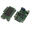
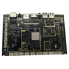
- Изготовление печатной платы:
- Двусторонняя печатная плата толщиной 2,4 мм., 1-2Оз меди, Загадка финишировать, и термический благодаря конструкции для отвода тепла.
- Компоненты Аутсорсинг:
- Приобретение сертифицированных комплектующих. (конденсаторы, МОП-транзисторы, IGBTS) от уполномоченных дистрибьюторов, обеспечение прослеживаемости.
- Пост&THT интеграция:
- Сборка смешанной технологии поддерживает мощные устройства (НАПРИМЕР., БТИЗ-модули) и микросхемы с мелким шагом.
- Тестирование & Сертификация:
- Соответствие МЭК 61727 (солнечные инверторы), UL 1973 (накопитель энергии), и ISO 9001:2015.
- Солнечные инверторы: PCBA для струнных инверторов, центральные инверторы, и микроинверторы с управлением MPPT.
- Системы управления батареями (БМС): Высоковольтная BMS для массивов накопления энергии и аккумуляторных блоков электромобилей.
- Зарядные станции для электромобилей: Силовая электроника для устройств быстрой зарядки постоянного тока (60кВт-150кВт) и модули зарядки переменного тока.
- Органы управления ветряными турбинами: Пульты управления системами подачи, преобразовательные блоки, и мониторинг состояния.