
Полностью Hong Electronics Co., ООО.
МЕНЮ

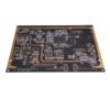
Категория: Печатная плата
Информация о продукте
Тип печатной платы
4L FR4 TG170 Плата
Толщина доски
1.6мм
Толщина меди
Все слои 1 унции
Припаяя маска
Черный
Поверхностная обработка
Соглашаться
Ключевые функции
BGA поддержка, Набросок маршрутизации
Сертификация & Приложение
IATF16949 Сертифицирован, Подходит для автомобильного поля
Процесс изготовления печатной платы
Внутренний слой — Сверлить — Пт & Панель — Сухая пленка — Контакт — Развивать — Перекрытие с шаблоном — Оловянное покрытие — Сухой пленочная полоса — Травление — Оловянная полоса — Припаяя маска — Поверхностная отделка — Электронный тест
Эта 4-слойная печатная плата FR4 TG170 представляет собой высоконадежную электронную подложку, разработанную с учетом строгих требований автомобильной промышленности., подтверждено сертификацией IATF16949. Разработан для самых разных приложений: от передовых систем помощи водителю. (Адас) для бортовой информационно-развлекательной системы и управления трансмиссией, печатная плата сочетает в себе термическую стабильность, целостность сигнала, и механическая прочность для работы в суровых автомобильных условиях..
1. Термическая стабильность & Превосходство материалов
Построенный из материала FR4 с температурой стеклянной перехода (Тг) 170 ° C., эта печатная плата превосходит стандарт FR4 (Тг130°С) в условиях высоких температур, например, установка под капотом или длительная эксплуатация в экстремальных климатических условиях.. Толщина 1,6 мм обеспечивает оптимальную механическую жесткость, позволяющую противостоять вибрациям автомобиля. (5-500Гц) и потрясения, в то время как 1 унция (35мкм) медь на всех слоях обеспечивает надежную обработку тока (до 8А на трассу) и эффективный отвод тепла через тепловые переходы. Это делает его идеальным для автомобильных применений, где управление температурным режимом имеет решающее значение., например, контроллеры двигателей, системы управления батареями (БМС), и светодиодные модули освещения.
2. Улучшенная обработка поверхности & Особенности конструкции
- Загадочная поверхность отделка:
Электролетное никелевое погружение (Соглашаться) Отделка обеспечивает барьерный слой никеля толщиной 3–5 мкм для предотвращения коррозии меди., в сочетании со слоем золота толщиной 0,05-0,1 мкм для превосходной паяемости и соединения проводов. Это обеспечивает долгосрочную надежность вставных разъемов и компонентов с малым шагом. (до 0,5 мм BGA), даже во влажной или агрессивной среде, типичной для салона и экстерьера автомобиля. - Черная паяльная маска LPI:
Черная паяльная маска не только повышает визуальный контраст для точного размещения компонентов и доработки, но также обеспечивает устойчивость к ультрафиолетовому излучению., защита платы от деградации в местах, подверженных воздействию солнечных лучей, таких как датчики на крыше или модули наружного освещения.. Его химическая стойкость к автомобильным жидкостям. (НАПРИМЕР., масла, охлаждающие жидкости) еще больше продлевает срок службы печатной платы. - BGA-совместимость & Набросок маршрутизации:
Печатная плата поддерживает решетку шариков. (BGA) компоненты с оптимизированной панелью via-in-pad (VIP) дизайн и микроотверстия, просверленные лазером, обеспечение полостей в паяных соединениях и минимальной индуктивности для высокоскоростных сигналов (НАПРИМЕР., CAN ФД, Ethernet). Точная контурная маршрутизация (Допуск ±0,1 мм) создает гладкий, края без заусенцев для бесшовной интеграции в специальные автомобильные корпуса, сокращение времени установки и улучшение механической посадки.
3. Производственный процесс, соответствующий стандарту IATF16949
Печатная плата проходит строгий процесс изготовления, соответствующий автомобильным стандартам качества.:
- Обработка внутреннего слоя:
Лазерная прямая визуализация (LDI) определяет структуру линий/пространств размером 100 мкм на медных жилах толщиной 1 унция, с последующим травлением для формирования сигнальных и силовых/земляных плоскостей. Автоматическая оптическая проверка (Аои) проверяет выравнивание слоев в пределах ±50 мкм. - Бурение & Покрытие:
Высокоточное механическое сверление создает отверстия с точностью ±50 мкм., которые затем покрываются химическим и электролитическим медным покрытием. (35Общая толщина мкм) для надежного соединения через отверстия. - Поверхностная отделка & Сборка:
Процесс ENIG обеспечивает равномерное наплавление металла., в то время как черная паяльная маска отверждается при температуре 150°C для обеспечения химической стойкости.. Каждая доска подвергается 100% Электрические испытания (Электронный тест) для преемственности (≤0,1o) и изоляция (≥100 МОм), с рентгеновским контролем для проверки целостности BGA. Панели X-out строго отвергаются. для устранения дефектов.
4. Автомобильные приложения & Надежность
- Адас & Сенсорные модули:
Поддерживает высокую плотность интеграции радаров/лидарных датчиков., процессоры изображений, и инерционные единицы измерения (ИДУ), с контролируемым сопротивлением (50Ω ± 8%) для передачи сигналов с малой задержкой в системах безопасности реального времени. - Блоки управления силовым агрегатом (КПСС):
Обеспечивает переключение сильноточной мощности (НАПРИМЕР., Драйверы БТИЗ) и низкоскоростные сигналы управления, с тепловыми переходами, снижающими температуру горячих точек на 15°C на силовых ступенях. - Автомобильная информационно-развлекательная система (ИВИ):
Обеспечивает плавную интеграцию контроллеров сенсорного экрана., аудиопроцессоры, и беспроводные модули, с подавлением электромагнитных помех из 4-слойного стека (2 Слои сигнала + 2 наземные/силовые плоскости). - Телематика & Возможности подключения:
Поддерживает коммуникационные модули 5G/CAN/LIN., обеспечение надежной передачи данных по беспроводной сети (ОТА) обновления и автомобиль ко всему (V2X) возможность подключения.
5. Гарантия качества & Согласие
- Сертификация IATF16949:
На производстве действуют строгие системы управления качеством автомобильной промышленности., обеспечение прослеживаемости материалов (НАПРИМЕР., Медь, соответствующая RoHS, бессвинцовый ЭНИГ) и последовательность процесса. - Экологические испытания:
Термический велосипед (-40° C до +85 ° C., 1,000 цикл) и тестирование влажности (85% относительной влажности, 1,000 часы) проверить устойчивость печатной платы в условиях эксплуатации автомобилей.
Объединив тепловые характеристики TG170, Загадочная надежность, и соответствие IATF16949, Эта 4-слойная печатная плата представляет собой экономичное, но высокопроизводительное решение для автомобильной электроники средней сложности.. Его способность балансировать плотность, тепловое управление, и целостность сигнала делают его важным компонентом для OEM-производителей и Tier 1 поставщики разрабатывают следующее поколение интеллектуальных, безопасный, и подключенные транспортные средства. Используется ли в ADAS, органы управления трансмиссией, или информационно-развлекательные системы, эта печатная плата обеспечивает надежность, необходимую для критически важных автомобильных приложений..
Более
Более