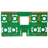
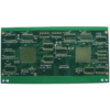
8-layer BGA Gold Finger FR4 PCB is designed for mission-critical applications demanding both high-density component integration and robust electrical connectivity, such as industrial automation controllers, medical diagnostic equipment, and aerospace avionics. 그만큼 8-layer structure (typically 4 신호 레이어 + 4 전원/지상 비행기) enables complex routing for fine-pitch BGAs while maintaining signal integrity through dedicated power and ground planes. 그만큼 2.0mm board thickness provides mechanical stability for applications subject to vibration or thermal cycling, ensuring long-term reliability.


A key feature is the 0.25mm plugged vias, which allow for precise via-in-pad construction under BGAs, eliminating the risk of solder wicking and ensuring reliable connections for high-density components. 그만큼 0.1mm minimum solder dam enhances soldering precision, preventing bridging between adjacent pads—a critical requirement for miniaturized designs. 그만큼 동의하다 (전기 전기 니켈 몰입 금) surface treatment on the PCB’s circuitry provides a smooth, corrosion-resistant finish that promotes excellent solderability, 동안 gold plated fingers (typically 1-3μm gold thickness) offer superior conductivity and wear resistance for edge connector applications, such as backplane interfaces or high-speed data ports.


The manufacturing process combines advanced techniques to ensure precision and quality:


  • Sequential lamination creates the 8-layer stackup with precise alignment of internal layers.
  • Microvia drilling achieves 0.25mm vias with ±5μm accuracy, essential for fine-pitch BGA designs.
  • Selective gold plating on the fingers ensures uniform thickness and adhesion, while ENIG is applied to the rest of the board.
  • 3D AOI inspection verifies solder dam integrity and via plugging, while X-ray inspection confirms internal via quality.


Engineers will appreciate the board’s versatility in handling both high-density components (예를 들어, 0.4mm pitch BGAs) and robust edge connectors. In industrial applications, it supports high-speed communication interfaces (such as CANbus or EtherCAT) while withstanding harsh environments. In medical devices, its reliability and precision meet the strict requirements for diagnostic equipment. In aerospace, the gold plated fingers provide stable connections in environments prone to vibration and temperature extremes.


By choosing this 8-layer BGA Gold Finger PCB, customers gain a solution that balances advanced component integration with reliable edge connectivity. Its combination of 0.25mm plugged vias, 0.1mm solder dams, and dual surface treatments (동의하다 + gold plated fingers) makes it a strategic choice for applications where both component density and connection durability are critical. ISO에 의해 지원됩니다 9001:2015 certification and IPC-6012 Class 2/3 compliance (optional), this PCB ensures consistent performance from prototype to mass production.

PCB 기능


표준 PCB 맞춤형 PCB
레이어 수 2-20 2-50
재료 FR4 대만 연합의 고속 재료, 그리고 기술, Rogers 등의 고주파 재료.
PCB 두께 0.4-3.2mm 0.4-6.4mm
구리 중량 가져 오기 -3o 가져 오기 10
최소. 구멍 직경 0.3mm 0.1레이저 드릴에 의한 MM
PCB 크기 최소. 6.00x6.00mm 최대. 600.00x620.00mm
PCB 마감 할, Hal-Leadfree, 동의하다, Enepic, 침지 주석, 침수은, OSP
Min.Soldermask 댐. 41oz에 대한 MILS 2.51oz에 대한 MILS
Prepreg 유형 2116,1080 2116,1080,7628,3313,106
Min.Width/Space 4/4 밀스 2.5/2.5 밀스
최소. 환형 반지 4/4 밀스 2.5/2.5 밀스
종횡비 8:1 15:1
리드 타임 2 주 5 날 - 5 주
임피던스 공차 ±5% - ±10% ±5% - ±10%
다른 기술 금 손가락, 맹인과 묻힌 구멍, 껍질을 벗길 수있는 솔더 마스크, 가장자리 도금, 카본 마스크, 카운터 싱크 구멍,
반/카스텔 화 구멍, Fit Hole을 누릅니다, 수지로 꽂고 채워진 것을 통해, 패드를 통해 (요일, POFV), 하나의 PCB에서 다재다능합니다

이것은 닫힙니다 0

PCBA 기능


아니요. 프로세스 기능 매개 변수
1 주문 수량 1pc 이상
2 PCB 유형 강성 PCB, FPC, RIDID-FLEX PCB
3 어셈블리 기술 smt, tht, 혼합 기술 또는 팝
4 구성 요소 소싱 완전한 턴키, 부분적인 턴키, 위탁
5 PCB 크기 45*45mm -- 510*500mm
6 BGA 패키지 bga 그녀. 0.14mm, BGA 0.2mm 피치
7 부품 프레젠테이션 줄자, 릴, 스틱 또는 트레이
8 철사 & 케이블 와이어 하네스 및 케이블 어셈블리
9 품질 검사 시각적, SPI, FAI, AOI; 엑스선 점검
10 장착 정확도 ±0.035mm (±0.025mm)
11 최소 패키지 01005 (0.4mm*0.2mm)
12 적합성 코팅 머신에서 사용할 수 있습니다
13 IC 검사 기능, 전기 또는 삭제 테스트
14 리드 타임 3 날 - 5 주
15 다른 기술 박스 빌드 어셈블리, IC 프로그래밍, 구성 요소 비용 다운, 기능 & 노화 테스트 커스텀으로서,
Fit Assembly를 누릅니다, SAC305 또는 더 나은 솔더 페이스트 사용, BGA realling 또는 재 작업,
EMI 방출 제어를위한 방패 덮개 어셈블리

이것은 닫힙니다 0

FPC 기능


아니요. 프로세스 기능 매개 변수
1 레이어 수 1-8 레이어
2 FPC 자료 pi, 애완 동물, 펜, FR-4
3 최종 두께 0.06-4.0mm
4 보드 크기 250.00x1200mm
5 구리 호일 12하나,18하나,35하나,70하나
6 최소 폭/공간 3천/3mil
7 홀로 볼 구리 두께 8-20μm
8 표면 처리 홀 리드 드리, 동의하다, 몰입은/주석, OSP
9 차원을 개요합니다 ± 2mil
10 솔더 내열 저항 280℃ / 10SECS
11 보강재 유형 pi, FR4, 스테인레스 스틸, 알류미늄
12 최소. 홀 데이 (PTH) 0.1mm ± 3mils
13 최소. 홀 데이 (npth) 0.25± 2mil
14 최대/최소 솔더 마스크 두께 2MIL/0.5mil (501/12.7um)
15 최소 슬롯 0.8mm × 1mm

이것은 닫힙니다 0