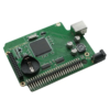
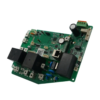
This 2-layer FR4 PCB addresses the needs of industrial automation, sensor networks, and power management applications requiring a balance of compact design and robust performance. With dimensions of 100×79.69mm and a 1.6MM 두께, the board offers a versatile platform for integrating microcontrollers, communication interfaces, and power components in a space-efficient form factor. Constructed from FR4 material, it ensures stable electrical insulation (dielectric constant εr=4.5) and mechanical rigidity, suitable for operation in moderate-temperature industrial environments with minimal vibration.

Layer Architecture & Electrical Design

  • 2-Layer Stackup:
    • Top and bottom signal layers with ground/power planes implemented via copper pours, reducing electromagnetic interference (에미) for basic signal integrity.
    • Split power domains (예를 들어, 5V/3.3V) separated by isolation traces to minimize cross-talk between analog and digital sections.
  • 1온스 (35μm) 구리 두께:
    • Supports up to 8A current in power traces (≥1mm width) for motor drivers or solenoid valves.
    • Enables fine-line routing (최소 선/공간: 100µm/100mm) for low-speed signals (UART, I2C) and component density.

Industrial-Grade Features

  • 녹색 LPI 솔더 마스크:
    • Standard industrial color for easy visual inspection during assembly and maintenance.
    • Chemical resistance against oils, 냉각제, and cleaning agents common in manufacturing environments.
  • ENIG Surface Finish:
    • 3–5μm nickel layer for corrosion protection; 0.05–0.1μm gold layer ensures reliable solderability for both SMT and DIP components, even after long-term storage.
  • SMT+DIP Mixed Assembly:
    • smt: Accommodates 0402 passive components, SOIC/SSOP ICs, and 0.5mm pitch QFP packages for high-density integration.
    • DIP: Supports through-hole connectors (예를 들어, 0.1″ headers, terminal blocks) and relays for robust field wiring in industrial setups.

Manufacturing & 품질 관리

  • Precision Fabrication:
    • Laser direct imaging (LDI) for 100μm trace accuracy, ensuring consistent routing across the board.
    • Electrolytic copper plating with uniform thickness verification to maintain conductivity.
  • Comprehensive Testing:
    • 100% automated optical inspection (AOI) to verify solder mask coverage and silkscreen clarity.
    • Flying probe testing for electrical continuity (≤0.1o) 그리고 격리 (≥100mΩ) to eliminate open/short circuits.
    • 열 응력 테스트 (260° C 반사 사이클) to ensure solder joint reliability during assembly.
  • Standards Compliance:
    • Meets IPC-6012 Class 2 standards for industrial electronics.
    • ROHS/REACH는 무연 및 위험 물질 제한을 준수합니다.

Industrial Applications

  • Industrial Sensor Modules:
    Integrates temperature, humidity, or pressure sensors with analog signal conditioning and wireless communication (예를 들어, LoRa, BLE).
  • Motor Control Units:
    Drives low-voltage DC motors in conveyor systems, featuring PWM control, current limiting, and overheat protection.
  • Communication Interfaces:
    Enables protocol conversion (예를 들어, RS-485 to USB) for legacy industrial equipment integration with modern control systems.
  • Power Distribution Panels:
    Manages 24V DC power distribution to multiple loads, with circuit protection (fuses, TVS diodes) and status indication LEDs.

PCB 기능


표준 PCB 맞춤형 PCB
레이어 수 2-20 2-50
재료 FR4 대만 연합의 고속 재료, 그리고 기술, Rogers 등의 고주파 재료.
PCB 두께 0.4-3.2mm 0.4-6.4mm
구리 중량 가져 오기 -3o 가져 오기 10
최소. 구멍 직경 0.3mm 0.1레이저 드릴에 의한 MM
PCB 크기 최소. 6.00x6.00mm 최대. 600.00x620.00mm
PCB 마감 할, Hal-Leadfree, 동의하다, Enepic, 침지 주석, 침수은, OSP
Min.Soldermask 댐. 41oz에 대한 MILS 2.51oz에 대한 MILS
Prepreg 유형 2116,1080 2116,1080,7628,3313,106
Min.Width/Space 4/4 밀스 2.5/2.5 밀스
최소. 환형 반지 4/4 밀스 2.5/2.5 밀스
종횡비 8:1 15:1
리드 타임 2 주 5 날 - 5 주
임피던스 공차 ±5% - ±10% ±5% - ±10%
다른 기술 금 손가락, 맹인과 묻힌 구멍, 껍질을 벗길 수있는 솔더 마스크, 가장자리 도금, 카본 마스크, 카운터 싱크 구멍,
반/카스텔 화 구멍, Fit Hole을 누릅니다, 수지로 꽂고 채워진 것을 통해, 패드를 통해 (요일, POFV), 하나의 PCB에서 다재다능합니다

이것은 닫힙니다 0

PCBA 기능


아니요. 프로세스 기능 매개 변수
1 주문 수량 1pc 이상
2 PCB 유형 강성 PCB, FPC, RIDID-FLEX PCB
3 어셈블리 기술 smt, tht, 혼합 기술 또는 팝
4 구성 요소 소싱 완전한 턴키, 부분적인 턴키, 위탁
5 PCB 크기 45*45mm -- 510*500mm
6 BGA 패키지 bga 그녀. 0.14mm, BGA 0.2mm 피치
7 부품 프레젠테이션 줄자, 릴, 스틱 또는 트레이
8 철사 & 케이블 와이어 하네스 및 케이블 어셈블리
9 품질 검사 시각적, SPI, FAI, AOI; 엑스선 점검
10 장착 정확도 ±0.035mm (±0.025mm)
11 최소 패키지 01005 (0.4mm*0.2mm)
12 적합성 코팅 머신에서 사용할 수 있습니다
13 IC 검사 기능, 전기 또는 삭제 테스트
14 리드 타임 3 날 - 5 주
15 다른 기술 박스 빌드 어셈블리, IC 프로그래밍, 구성 요소 비용 다운, 기능 & 노화 테스트 커스텀으로서,
Fit Assembly를 누릅니다, SAC305 또는 더 나은 솔더 페이스트 사용, BGA realling 또는 재 작업,
EMI 방출 제어를위한 방패 덮개 어셈블리

이것은 닫힙니다 0

FPC 기능


아니요. 프로세스 기능 매개 변수
1 레이어 수 1-8 레이어
2 FPC 자료 pi, 애완 동물, 펜, FR-4
3 최종 두께 0.06-4.0mm
4 보드 크기 250.00x1200mm
5 구리 호일 12하나,18하나,35하나,70하나
6 최소 폭/공간 3천/3mil
7 홀로 볼 구리 두께 8-20μm
8 표면 처리 홀 리드 드리, 동의하다, 몰입은/주석, OSP
9 차원을 개요합니다 ± 2mil
10 솔더 내열 저항 280℃ / 10SECS
11 보강재 유형 pi, FR4, 스테인레스 스틸, 알류미늄
12 최소. 홀 데이 (PTH) 0.1mm ± 3mils
13 최소. 홀 데이 (npth) 0.25± 2mil
14 최대/최소 솔더 마스크 두께 2MIL/0.5mil (501/12.7um)
15 최소 슬롯 0.8mm × 1mm

이것은 닫힙니다 0