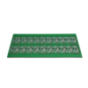
Esta PCB FR4 TG170 de 6 capas está diseñada para aplicaciones de alta confiabilidad, incluida la automatización industrial., 5comunicación g, y dispositivos médicos. Con un espesor de 1,6 mm y 1 oz de cobre en todas las capas., Garantiza una excelente estabilidad térmica e integridad de la señal.. El acabado superficial ENIG mejora la soldabilidad y la durabilidad a largo plazo..
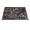
Con 4 capas de señal y 2 planos de potencia/tierra dedicados, Esta PCB admite enrutamiento de impedancia controlada (50Ω ±8%). Minimiza las interferencias electromagnéticas. (EMI) y permite velocidades de transferencia de datos de hasta 10 Gbps, ideal para USB 3.0, Éternet, y señales de alta frecuencia.
Acabado superficial de enig: Proporciona resistencia a la corrosión y excelente soldabilidad., admite componentes de paso fino de hasta BGA de 0,5 mm de paso.
Máscara de soldadura LPI negra: Ofrece resistencia química y a los rayos UV., ideal para ambientes exteriores e industriales.
Contactos de dedo dorado: Garantiza durabilidad, conexiones de baja resistencia en sistemas modulares con revestimiento preciso (2µin de oro).
Enrutamiento de contorno de precisión: Mantiene tolerancias mecánicas estrictas. (±0,1 mm) para cerramientos personalizados.
Nuestro proceso de fabricación incluye imágenes directas con láser., perforación de alta precisión, revestimiento no electrolítico, y 100% prueba eléctrica. Inspección óptica automatizada (AOI) y las comprobaciones de rayos X garantizan PCB libres de defectos que cumplen con la clase IPC-6012 2 estándares.
Automatización Industrial: Soporta PLC, unidades de motor, y puertas de enlace de IoT con potencia estable y comunicación rápida.
5GRAMO & Comunicación inalámbrica: Mantiene la integridad de RF para módulos sub-6GHz y Wi-Fi 6 dispositivos.
Dispositivos médicos: Cumple con RoHS y REACH, Adecuado para equipos portátiles y de diagnóstico..
Aeroespacial & Defensa: Resiste temperaturas y vibraciones extremas para uso en aviónica..