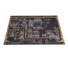
Diese 4-layerer FR4 TG170-LCB ist ein elektronisches Substrat mit hoher Zuverlässigkeit, das die strengen Anforderungen der Automobilindustrie entspricht, unterstützt durch IATF16949 Zertifizierung. Entwickelt für Anwendungen, die von fortschrittlichen Fahrerassistanzsystemen reichen (Adas) zu Infotainment- und Antriebsstrangkontrolle im Fahrzeug, Die PCB kombiniert die thermische Stabilität, Signalintegrität, und mechanische Robustheit, in der harten Automobilumgebung zu gedeihen.
Aus FR4 -Material mit einer Glasübergangstemperatur gebaut (Tg) von 170 ° C., Diese PCB übertrifft Standard FR4 (TG130 ° C.) In Hochtemperaturszenarien, wie unter den Hausanlagen oder längerer Betrieb in extremen Klimazonen. Die 1,6 -mm -Dicke sorgt für eine optimale mechanische Steifheit, um Fahrzeugvibrationen zu widerstehen (5-500Hz) und Schocks, während der 1oz (35μm) Kupfer auf allen Schichten sorgt für eine zuverlässige aktuelle Handhabung (bis zu 8a pro Spur) und effiziente Wärmeabteilung durch thermische Vias. Dies macht es ideal für Automobilanwendungen, bei denen das thermische Management kritisch ist, wie motorische Controller, Batteriemanagementsysteme (BMS), und LED -Beleuchtungsmodule.
- Rätseloberfläche:
Das elektrolololose Nickel -Eintauchgold (Zustimmen) Finish liefert eine 3-5 & mgr; m-Nickel-Barrier-Schicht, um Kupferkorrosion zu verhindern, kombiniert mit einer Goldschicht von 0,05-0,1 μm für überlegene Lötlichkeit und Drahtbindung. Dies gewährleistet eine langfristige Zuverlässigkeit von Steckbetrieben und Feinkopienkomponenten (bis 0,5 mm BGA), Auch in feuchten oder korrosiven Umgebungen, die für Automobilverkehrs- und Außenbereiche typisch sind.
- Black LPI Lötmaske:
Die schwarze Lötmaske verbessert nicht nur den visuellen Kontrast für die Platzierung und Nacharbeit der Komponenten, sondern bietet auch UV -Widerstand, Schutz des Boards vor Abbau in sonnenverletzten Bereichen wie Dachsensoren oder Außenbeleuchtungsmodulen. Seine chemische Resistenz gegen Automobilflüssigkeiten (Z.B., Öle, Kühlmittel) Erweitert die Lebensdauer der PCB weiter.
- BGA -Kompatibilität & Umriss Routing:
Die PCB unterstützt das Ballgitterarray (BGA) Komponenten mit optimiertem VIC-in-Pad (VIP) Design- und Lasermikrovias, Gewährleistung von Lötverbindungen freier freier Lötverbeine und minimaler Induktivität für Hochgeschwindigkeitssignale (Z.B., Kann fd, Ethernet). Präzisionsumrisse Routing (± 0,1 mm Toleranz) schafft glatt, burr-freie Kanten für die nahtlose Integration in benutzerdefinierte Automobilgehäuse, Verringerung der Installationszeit und Verbesserung der mechanischen Anpassung.
Die PCB erfährt einen strengen Herstellungsprozess, der mit den Standards der Automobilqualität entspricht:
- Innenschichtverarbeitung:
Laser Direct Imaging (LDI) Definiert 100 & mgr; m Linien-/Raummuster auf 1oz Kupferkernen, gefolgt von Ätzen, um Signal- und Strom-/Bodenebenen zu bilden. Automatisierte optische Inspektion (Aoi) Überprüft die Schichtausrichtung innerhalb von ± 50 μm.
- Bohren & Überzug:
Mechanische Bohrungen mit hoher Präzision erzeugen VIAS mit ± 50 μm Genauigkeit, die dann mit elektrolarischem und elektrolytischem Kupfer plattiert werden (35μm Gesamtdicke) Für eine robuste Durchleitungskonnektivität.
- Oberflächenbeschaffung & Montage:
Der Enig -Prozess sorgt für eine gleichmäßige Metallabscheidung, Während die schwarze Lötmaske bei 150 ° C zur chemischen Resistenz geheilt wird. Jeder Vorstand unterzieht sich 100% elektrische Tests (E-Test) Für Kontinuität (≤ 0,1o) und Isolation (≥100 mΩ), Mit Röntgeninspektion zur Validierung von BGA über Integrität. X-Out-Panels werden streng abgelehnt Defekte beseitigen.
- Adas & Sensormodule:
Unterstützt die Integration von Radar-/Lidar-Sensoren mit hoher Dichte, Bildprozessoren, und Trägheitsmesseinheiten (Imus), mit kontrollierter Impedanz (50Ω ± 8%) Bei Signalübertragung mit niedriger Latenz in Echtzeitsicherheitssystemen.
- Antriebsstrangsteuereinheiten (CPSU):
Verarbeitet Hochstrom-Stromschaltungen (Z.B., IGBT -Treiber) und Kontrollsignale mit niedriger Geschwindigkeit, Mit thermischen Vias reduzieren die Hotspot -Temperaturen um 15 ° C in Leistungsstadien.
- In-Vehicle-Infotainment (IVI):
Ermöglicht eine nahtlose Integration von Touchscreen -Controllern, Audioprozessoren, und drahtlose Module, mit EMI-Unterdrückung aus dem 4-Schicht-Stackup (2 Signalschichten + 2 Boden-/Kraftebenen).
- Telematik & Konnektivität:
Unterstützt 5G/CAN/Lin -Kommunikationsmodule, Gewährleistung der zuverlässigen Datenübertragung für regelmäßige Luft (Ota) Updates und Fahrzeug-zu-alles-alles (V2x) Konnektivität.
- IATF16949 Zertifizierung:
Die Produktionsstätte hält strenge Systeme für die Automobilqualitätsmanagementsysteme an, Sicherstellung der Rückverfolgbarkeit von Materialien (Z.B., ROHS-konforme Kupfer, Lead-Free-Rätsel) und Prozesskonsistenz.
- Umwelttests:
Thermalradfahren (-40° C bis +85 ° C., 1,000 Zyklen) und Feuchtigkeitstests (85% Rh, 1,000 Std.) Überprüfen Sie die Resilienz der PCB unter den Betriebsbedingungen für Automobile.
Durch Kombination von TG170 Wärmeleistung, REIG -Zuverlässigkeit, und IATF16949 Compliance, Diese 4-layer-PCB bietet eine kostengünstige und dennoch Hochleistungslösung für die Mid-Komplexitäts-Automobilelektronik. Seine Fähigkeit, die Dichte auszugleichen, Thermalmanagement, und Signalintegrität macht es zu einer wesentlichen Komponente für OEMs und Stufe 1 Lieferanten, die die nächste Generation von Smart entwickeln, sicher, und verbundene Fahrzeuge. Ob in ADAS verwendet, Antriebsstrangsteuerung, oder Infotainment -Systeme, Diese PCB liefert die Zuverlässigkeit, die für missionskritische Automobilanwendungen erforderlich ist.