
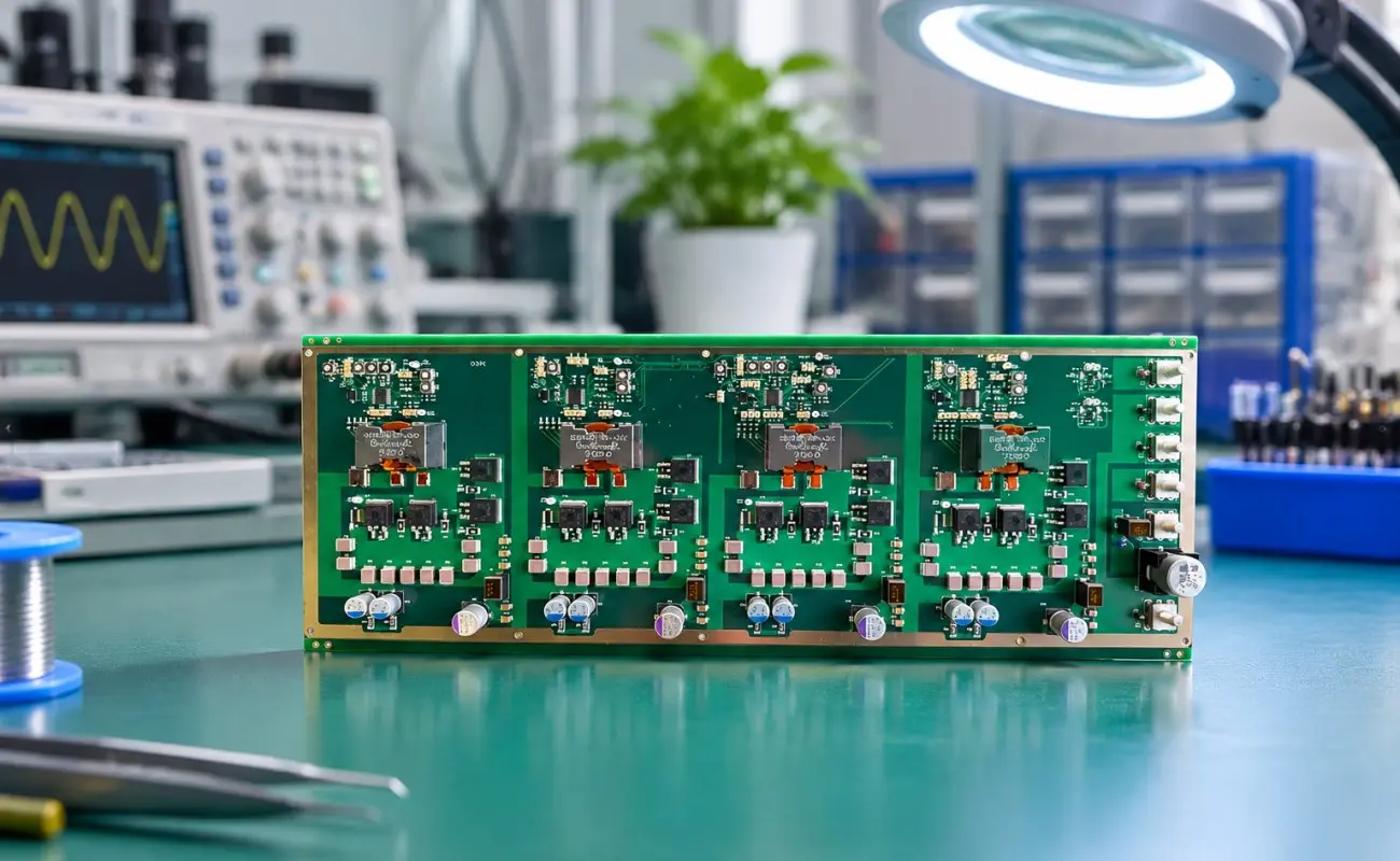
Industrial control systems operate in environments where electrical noise, temperature fluctuations, and mechanical vibration can affect circuit performance. Meanwhile, control boards often need to integrate microcontrollers, signal conditioning circuits, relays, motor drivers, and field connectors within a single assembly. A 4-layer industrial control PCB assembly helps address these challenges through dedicated signal, power, and ground layers. However, achieving stable signal integrity also requires careful attention to PCB layout, grounding, component placement, and surface protection.
How Does a Four-Layer Stackup Improve Signal Integrity?
A four-layer PCB provides more routing flexibility than a basic two-layer board because designers can distribute electrical functions across multiple copper layers. The described industrial control board uses two signal layers and two power or ground planes. This arrangement provides dedicated paths for signal routing and power distribution, while the inner reference planes help control electromagnetic interference (EMI). In addition, a structured stackup can reduce unnecessary routing complexity and support more organized connections between control components.
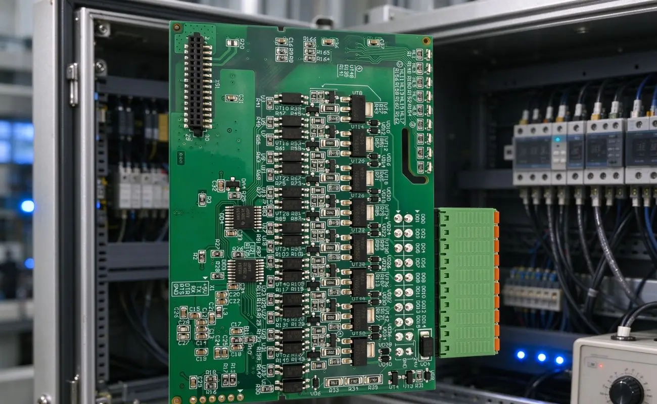
The board uses FR4 material with a dielectric constant of approximately 4.5 and a thickness of 1.5 mm. Its 350 × 125 mm dimensions provide space for integrating larger components, relays, and connectors in industrial control cabinets. Furthermore, the 1 oz (35 μm) copper thickness supports moderate current requirements, with the supplied design specifying up to 10A per trace. Designers should still verify trace width, copper temperature rise, and operating conditions before finalizing current-carrying paths.
Tip 1: Separate Signal Routing from Power Distribution
Power circuits and signal circuits have different electrical requirements. Motor drivers, solenoid valves, and other power-demanding devices can introduce switching noise that affects nearby control signals. Therefore, separating power distribution from sensitive signal routing is an important step when designing industrial control boards. Dedicated power and ground planes can help organize current paths and provide more consistent reference connections for signal circuits.
For this board, the inner power planes are optimized for 24V DC distribution. Copper pour areas can also help reduce resistive heating by providing additional conductive area for power connections. Nevertheless, designers should avoid routing sensitive signals through areas with significant switching activity whenever possible. They should also review return-current paths to prevent unnecessary interference between power and signal sections. A 4-layer industrial control PCB assembly also benefits from this separation because dedicated power and ground planes help organize electrical paths and reduce unwanted signal interference.
Tip 2: Optimize Grounding and EMI Control
A well-planned grounding structure helps reduce unwanted electrical noise and maintain stable signal references. In a multilayer PCB manufacturing process, designers should consider how ground planes connect to signal traces, connectors, and high-speed or noise-sensitive components. Continuous reference planes can provide more predictable return paths, while poorly planned splits or gaps may force current to follow longer routes. Consequently, grounding decisions should be evaluated together with the complete circuit layout rather than treated as a final routing detail.
Practical EMI control measures include:
- Maintain clear separation between sensitive signal paths and noisy power circuits.
- Use continuous ground reference areas wherever the design allows.
- Keep switching power components and their current loops away from sensitive control signals.
- Place decoupling capacitors close to the power pins of relevant ICs.
- Review connector grounding and cable entry points to reduce external noise coupling.
These measures can help improve electromagnetic compatibility, although final performance depends on the complete circuit, enclosure, cabling, and operating environment. Therefore, prototype testing under representative factory conditions remains important.
Tip 3: Choose an Appropriate ENIG PCB Finish
The PCB surface finish affects solderability, contact reliability, and protection of exposed copper. This design uses an ENIG PCB finish, which consists of a nickel layer and a thin gold layer. According to the supplied specifications, the nickel thickness is 3–5 μm, while the gold thickness is 0.05–0.1 μm. This finish helps protect exposed copper against corrosion and provides a suitable surface for soldering components and field-replaceable parts.
The board also uses a green liquid photoimageable (LPI) solder mask. Besides providing the familiar industrial PCB appearance, the specified solder mask offers resistance to oils, coolants, and cleaning agents. However, actual chemical compatibility depends on the substances, exposure duration, and operating conditions. For this reason, manufacturers should verify material suitability against the chemicals present in the intended installation environment.
Tip 4: Control Component Placement and Mixed Assembly
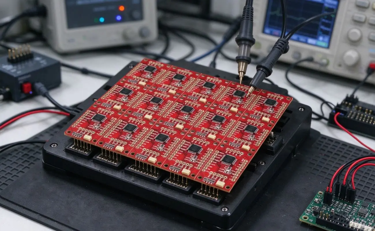
Component placement has a direct influence on signal routing, power distribution, and manufacturing quality. The board supports mixed SMT and DIP assembly, allowing designers to use surface-mounted components for compact electronic circuits and through-hole components for mechanical connections. For example, microcontrollers and signal conditioning ICs can be placed using SMT, while terminal blocks and DB9 ports can use through-hole mounting. This combination supports different connection and installation requirements within one control board.
The following practices can help improve layout and assembly consistency:
- Place signal conditioning components close to their related input or output interfaces.
- Keep power components and high-current paths organized to limit interference with sensitive signals.
- Position terminal blocks and DB9 connectors to support practical field wiring.
- Check component spacing and soldering access before PCB fabrication and assembly.
- Verify connector orientation and mechanical stability for cabinet installation.
By coordinating placement and assembly requirements early, designers can reduce avoidable layout conflicts and simplify production. In addition, reviewing the design for both electrical and mechanical requirements helps ensure that the finished board fits its intended control cabinet.
Key Specifications of the Industrial Control PCB
The following table summarizes the main construction and assembly details of this board. These specifications provide a starting point for evaluating electrical design, material selection, and manufacturing requirements.
| Parameter | Specification |
|---|---|
| PCB Structure | 4 Layers |
| Material | FR4 |
| Board Dimensions | 350 × 125 mm |
| Board Thickness | 1.5 mm |
| Dielectric Constant | εr = 4.5 |
| Copper Thickness | 1 oz / 35 μm |
| Layer Configuration | 2 Signal Layers + 2 Power/Ground Planes |
| Power Distribution | 24V DC |
| Specified Current Capacity | Up to 10A per trace |
| Solder Mask | Green LPI |
| Surface Finish | ENIG |
| Nickel Thickness | 3–5 μm |
| Gold Thickness | 0.05–0.1 μm |
| Assembly Type | SMT + DIP |
These parameters show how the board combines multilayer routing, power distribution, and mixed component assembly. However, current capacity and signal performance should always be assessed against actual trace geometry, circuit frequency, thermal conditions, and installation requirements.
Why Manufacturing Quality Matters in Industrial PCB Assembly
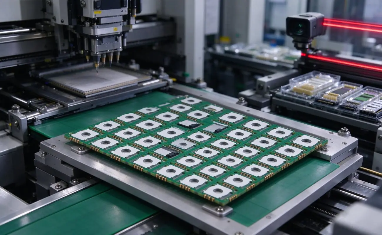
A reliable design also depends on consistent fabrication and assembly processes. Industrial PCB manufacturing involves material preparation, copper pattern formation, drilling, lamination, surface finishing, and electrical inspection. After fabrication, SMT PCB assembly and through-hole processes must follow the component placement and soldering requirements. Furthermore, inspection should cover solder joints, connector alignment, electrical continuity, and other project-specific acceptance criteria.
Fully Hong supports PCB fabrication and assembly requirements for industrial control applications. Coordinating fabrication specifications with assembly processes helps ensure that the finished board follows the intended design. Ultimately, a 4-layer industrial control PCB assembly can support demanding control applications when its stackup, grounding, surface finish, and component layout are properly engineered and verified.
Conclusion
Maintaining signal integrity in factory environments requires coordinated decisions throughout PCB design and manufacturing. A four-layer stackup provides dedicated routing and power distribution options, while careful grounding and component placement help manage electrical interference. In addition, ENIG finishing and suitable SMT/DIP assembly support the board’s connection and installation requirements. By applying these four design principles, manufacturers can develop industrial control boards with a more organized electrical layout and better suitability for their intended operating conditions. Therefore, a 4-layer industrial control PCB assembly should combine a suitable layer stackup, controlled power distribution, and carefully planned grounding to maintain reliable operation in factory environments.

Leave a reply