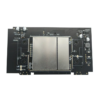
This 2-layer FR4 PCB addresses the needs of industrial control systems, automation modules, and power management applications requiring a balance of robust design and component integration. With dimensions of 140.45×93.72mm and a 2.0mm thickness, the board provides a stable platform for mounting microcontrollers, communication interfaces, and power components while maintaining mechanical rigidity for industrial environments. Constructed from FR4 material, it offers stable electrical insulation (dielectric constant εr=4.5) and mechanical strength, suitable for operation in environments with moderate temperature and vibration.

Layer Architecture & Power Design

  • 2-Layer Stackup:
    • Top and bottom signal layers with ground/power planes implemented via copper pours for basic EMI suppression
    • Split power domains (e.g., 5V/3.3V) separated by isolation traces to minimize cross-talk
  • 1OZ (35μm) Copper Thickness:
    • Supports moderate current loads (up to 8A per wide trace) for power-hungry components
    • Copper pour areas on both layers reduce thermal hotspots and improve power distribution

Industrial-Grade Features

  • Blue LPI Solder Mask:
    • Distinctive color for easy visual inspection and component identification in dense layouts
    • Chemical resistance against industrial contaminants and cleaning agents
  • ENIG Surface Finish:
    • 3–5μm nickel layer for corrosion resistance
    • 0.05–0.1μm gold layer for long-term solderability and wire bonding compatibility
  • Mixed SMT+DIP Capability:
    • SMT: High-density placement of 0402 passive components, SOIC/SSOP ICs, and 0.5mm pitch QFP packages
    • DIP: Through-hole mounting for rugged connectors (e.g., 0.1” headers, terminal blocks) and relays

Manufacturing & Quality Control

  • Precision Fabrication:
    • Laser direct imaging (LDI) for 100μm trace accuracy
    • Electrolytic copper plating with uniform thickness verification
  • Comprehensive Testing:
    • 100% automated optical inspection (AOI) for solder mask coverage and silkscreen clarity
    • Flying probe testing for electrical continuity (≤0.1Ω) and isolation (≥100MΩ)
    • Thermal cycling (-40°C to +85°C, 500 cycles) to verify reliability
  • Standards Compliance:
    • IPC-6012 Class 2 for industrial electronics
    • RoHS/REACH compliant for lead-free and hazardous substance restrictions

Industrial Applications

  • Industrial Sensor Modules:
    Integrates temperature/humidity sensors, analog-to-digital converters, and wireless modules (Zigbee/Bluetooth)
  • Motor Control Units:
    Manages low-voltage DC motors with PWM control, current sensing, and overheat protection
  • Communication Interfaces:
    Enables RS-232/485 to USB conversion or simple protocol bridges for industrial equipment
  • Power Distribution Blocks:
    Distributes 24V DC to multiple loads with circuit protection and status indication

PCB Capability


Item Standard PCB Customized PCB
Number of Layers 2-20 2-50
Material FR4 Hi Speed material from Taiwan Union, SY Tech, High Frequency material from Rogers etc.
PCB thickness 0.4-3.2mm 0.4-6.4mm
Copper Weight HOZ-3OZ HOZ-10OZ
Min. Hole Diameter 0.3mm 0.1mm by Laser Drill
PCB Size Min. 6.00X6.00mm Max. 600.00X620.00mm
PCB Finish HAL, HAL-leadfree, ENIG, ENEPIG, Immersion Tin, Immersion Silver, OSP
Min.Soldermask Dam. 4mils for 1OZ 2.5mils for 1OZ
Prepreg Type 2116,1080 2116,1080,7628,3313,106
Min.Width/Space 4/4 mils 2.5/2.5 mils
Min. Annular Ring 4/4 mils 2.5/2.5 mils
Aspect Ratio 8:1 15:1
Lead Time 2 weeks 5 Days - 5 Weeks
Impedance Tolerance ±5% - ±10% ±5% - ±10%
Other Techniques Gold fingers, Blind and Buried Holes, Peelable solder mask, Edge plating, Carbon Mask, Countersink hole,
Half/Castellated hole, Press fit hole, Via plugged/filled with resin, Via in pad (VIP, POFV), Multi-finishes on one PCB

This will close in 0 seconds

PCBA Capability


No. Item Process Capability Parameter
1 Order Quantity More than 1pcs
2 PCB Type Rigid PCB, FPC, Rigid-flex PCB
3 Assembly Tech SMT, THT, Mixed Tech or POP
4 Component Sourcing Full Turnkey, Partial Turnkey, Consigned
5 PCB Size 45*45mm -- 510*500mm
6 BGA Package BGA Dia. 0.14mm, BGA 0.2mm pitch
7 Parts Presentation Tape, Reel, Stick or Tray
8 Wire & Cable Wire harness and Cable Assembly
9 Quality Inspection Visual, SPI, FAI, AOI; X-RAY checking
10 Mounting Accuracy ±0.035mm (±0.025mm)
11 Min Package 01005 (0.4mm*0.2mm)
12 Conformal Coating Available by machine
13 IC Inspection Function, Electrical or Decap Test
14 Lead Time 3 days - 5 Weeks
15 Other Techniques Box Build Assembly, IC programming, Components cost-down, Function & aging test as custom,
Press fit assembly, SAC305 or better Solder Paste used, BGA reballing or rework,
Shield cover assembly for EMI emission control

This will close in 0 seconds

FPC Capability


No. Item Process Capability Parameter
1 Layer Count 1-8 Layers
2 FPC Material PI, PET, PEN, FR-4
3 Final Thickness 0.06-4.0mm
4 Board Size 250.00X1200mm
5 Copper Foil 12um,18um,35um,70um
6 Min width/Space 3mil/3mil
7 Holewall Copper Thickness 8-20μm
8 Surface Treatment HAL leadfree, ENIG, Immersion Silver/Tin, OSP
9 Outlines Dimension ±2mils
10 Solder Heat Resistance 280℃ / 10secs
11 Stiffener Type PI, FR4, Stainless Steel, Aluminum
12 Min. Hole Dia (PTH) 0.1mm±3mils
13 Min. Hole Dia (NPTH) 0.25±2mils
14 Max/Min Soldermask Thickness 2mil/0.5mil (50um/12.7um)
15 Min Slot 0.8mm×1mm

This will close in 0 seconds