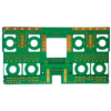
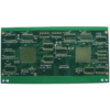
8-layer BGA Gold Finger FR4 PCB is designed for mission-critical applications demanding both high-density component integration and robust electrical connectivity, such as industrial automation controllers, medical diagnostic equipment, and aerospace avionics. Các 8-layer structure (typically 4 Lớp tín hiệu + 4 Máy bay điện/mặt đất) enables complex routing for fine-pitch BGAs while maintaining signal integrity through dedicated power and ground planes. Các 2.0Độ dày mm provides mechanical stability for applications subject to vibration or thermal cycling, ensuring long-term reliability.
A key feature is the 0.25mm plugged vias, which allow for precise via-in-pad construction under BGAs, eliminating the risk of solder wicking and ensuring reliable connections for high-density components. Các 0.1mm minimum solder dam enhances soldering precision, preventing bridging between adjacent pads—a critical requirement for miniaturized designs. Các Đồng ý (Điện phân Niken Vàng) surface treatment on the PCB’s circuitry provides a smooth, corrosion-resistant finish that promotes excellent solderability, Trong khi gold plated fingers (typically 1-3μm gold thickness) offer superior conductivity and wear resistance for edge connector applications, such as backplane interfaces or high-speed data ports.
The manufacturing process combines advanced techniques to ensure precision and quality:
- Sequential lamination creates the 8-layer stackup with precise alignment of internal layers.
- Microvia drilling achieves 0.25mm vias with ±5μm accuracy, essential for fine-pitch BGA designs.
- Selective gold plating on the fingers ensures uniform thickness and adhesion, while ENIG is applied to the rest of the board.
- 3D AOI inspection verifies solder dam integrity and via plugging, while X-ray inspection confirms internal via quality.
Engineers will appreciate the board’s versatility in handling both high-density components (ví dụ., 0.4mm pitch BGAs) and robust edge connectors. In industrial applications, it supports high-speed communication interfaces (such as CANbus or EtherCAT) while withstanding harsh environments. In medical devices, its reliability and precision meet the strict requirements for diagnostic equipment. In aerospace, the gold plated fingers provide stable connections in environments prone to vibration and temperature extremes.
By choosing this 8-layer BGA Gold Finger PCB, customers gain a solution that balances advanced component integration with reliable edge connectivity. Its combination of 0.25mm plugged vias, 0.1mm solder dams, and dual surface treatments (Đồng ý + gold plated fingers) makes it a strategic choice for applications where both component density and connection durability are critical. Được hỗ trợ bởi ISO 9001:2015 Chứng nhận và lớp IPC-6012 2/3 Tuân thủ (optional), PCB này đảm bảo hiệu suất nhất quán từ nguyên mẫu đến sản xuất hàng loạt.

")