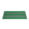
PCB FR4 TG170 6 lớp này được thiết kế cho các ứng dụng có độ tin cậy cao bao gồm tự động hóa công nghiệp, 5giao tiếp G, và thiết bị y tế. Có độ dày 1,6mm và đồng 1oz trên tất cả các lớp, nó đảm bảo độ ổn định nhiệt tuyệt vời và tính toàn vẹn tín hiệu. Bề mặt hoàn thiện ENIG tăng cường khả năng hàn và độ bền lâu dài.
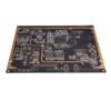
Với 4 lớp tín hiệu và 2 máy bay điện/mặt đất chuyên dụng, PCB này hỗ trợ định tuyến trở kháng được kiểm soát (50Ω ±8%). Nó giảm thiểu nhiễu điện từ (Emi) và cho phép tốc độ truyền dữ liệu lên tới 10Gbps, lý tưởng cho USB 3.0, Ethernet, và tín hiệu tần số cao.
Bề mặt hoàn thiện ENIG: Cung cấp khả năng chống ăn mòn và khả năng hàn tuyệt vời, hỗ trợ các thành phần có độ cao nhỏ tới BGA có độ cao tới 0,5mm.
Mặt nạ hàn LPI đen: Cung cấp khả năng chống tia cực tím và hóa chất, lý tưởng cho môi trường ngoài trời và công nghiệp.
Danh bạ ngón tay vàng: Đảm bảo độ bền, kết nối điện trở thấp trong các hệ thống mô-đun với lớp mạ chính xác (2μin vàng).
Định tuyến phác thảo chính xác: Duy trì dung sai cơ học chặt chẽ (± 0,1mm) cho các thùng tùy chỉnh.
Quá trình chế tạo của chúng tôi bao gồm hình ảnh trực tiếp bằng laser, khoan có độ chính xác cao, mạ điện, Và 100% thử nghiệm điện. Kiểm tra quang học tự động (Aoi) và kiểm tra bằng tia X đảm bảo PCB không có khuyết tật đáp ứng Lớp IPC-6012 2 tiêu chuẩn.
Tự động hóa công nghiệp: Hỗ trợ PLC, ổ đĩa động cơ, và cổng IoT với nguồn điện ổn định và tốc độ truyền thông nhanh.
5G & Truyền thông không dây: Duy trì tính toàn vẹn RF cho các mô-đun dưới 6GHz và Wi-Fi 6 thiết bị.
Thiết bị y tế: Tuân thủ RoHS và REACH, thích hợp cho thiết bị cầm tay và chẩn đoán.
Không gian vũ trụ & Phòng thủ: Chịu được nhiệt độ khắc nghiệt và độ rung khi sử dụng hệ thống điện tử hàng không.