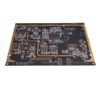
This 6-layer FR4 TG170 PCB is engineered for high-reliability applications including industrial automation, 5G-коммуникация, and medical devices. Featuring a 1.6mm thickness and 1oz copper on all layers, it ensures excellent thermal stability and signal integrity. The ENIG surface finish enhances solderability and long-term durability.
С 4 сигнальные слои и 2 dedicated power/ground planes, this PCB supports controlled impedance routing (50Ω ± 8%). It minimizes electromagnetic interference (Эми) and enables data transfer rates up to 10Gbps, ideal for USB 3.0, Ethernet, and high-frequency signals.
Загадочная поверхность отделка: Provides corrosion resistance and excellent solderability, supporting fine-pitch components down to 0.5mm pitch BGAs.
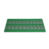
Черная паяльная маска LPI: Offers UV and chemical resistance, ideal for outdoor and industrial environments.
Gold Finger Contacts: Ensures durable, low-resistance connections in modular systems with precise plating (2μin gold).
Precision Outline Routing: Maintains tight mechanical tolerances (± 0,1 мм) for custom enclosures.
Our fabrication process includes laser direct imaging, high-precision drilling, electroless plating, и 100% Электрические испытания. Автоматическая оптическая проверка (Аои) and X-ray checks ensure defect-free PCBs that meet IPC-6012 Class 2 стандарты.
Industrial Automation: Supports PLCs, motor drives, and IoT gateways with stable power and fast communication.
5Г & Беспроводное общение: Maintains RF integrity for sub-6GHz modules and Wi-Fi 6 устройства.
Медицинские устройства: Compliant with RoHS and REACH, suitable for portable and diagnostic equipment.
Аэрокосмическая & Защита: Withstands extreme temperatures and vibrations for avionics use.