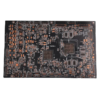
This 6-layer FR4 TG170 PCB delivers high performance for industrial automation, 5G communication modules, and other mission-critical electronics. Featuring a 1.6mm thickness, 1OZ copper on all layers, and an ENIG surface finish, it balances thermal stability, Integridad de señal, and mechanical durability effectively.
Because it uses FR4 material with a Tg of 170°C, this PCB withstands harsh industrial environments like factory floors, outdoor communication hubs, and automotive systems. Its 6-layer design includes 4 capas de señal y 2 aviones de potencia/terreno, which actively reduce electromagnetic interference (EMI). Por lo tanto, it ensures stable data transmission in applications such as PLCs, industrial IoT gateways, and wireless base stations.
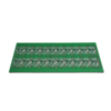
A key feature is the gold finger with 2 microinch plating, which provides excellent corrosion resistance and durable electrical contacts. This design suits systems requiring frequent board insertion/removal, including modular industrial systems and rack-mounted communication devices. Furthermore, the ENIG finish enhances solderability and wire bonding. It uses a nickel barrier to prevent oxidation and a thin gold layer optimized for fine-pitch components.
We apply a strict fabrication process to ensure precision and consistency:
Procesamiento de la capa interna: Imágenes directas láser (LDI) defines fine 75μm traces on 1OZ copper.
Perforación & Enchapado: Precision mechanical drilling and plated-through holes (Portalo) ensure robust electrical vias.
Outer Layer Patterning: Dry film lamination and tin plating protect circuitry during etching.
Acabado superficial: The ENIG coating combined with a green LPI solder mask enhances durability and visual clarity.
Control de calidad: We perform 100% prueba eléctrica (E-Test) and automated optical inspection (AOI) to guarantee defect-free boards. We strictly reject any X-out panels to maintain high quality.
Industrial Control Systems: Provide reliable power and signal integrity for PLCs and motor drives.
5GRAMO & Comunicación inalámbrica: Support RF integrity in 5G sub-6GHz and Wi-Fi 6 dispositivos.
Dispositivos médicos: Comply with RoHS/REACH and biocompatibility standards.
Aeroespacial & Defensa: Resist vibration and temperature cycling in rugged environments.
Estabilidad térmica: It outperforms standard FR4 and reduces delamination risk.
Reliable Gold Finger Contacts: Ensure low resistance and long-lasting performance.
Diseño flexible: Support mixed SMT/DIP assembly with fine-pitch compatibility.
Global Compliance: Meet IPC-6012 Class 2 quality standards for consistent mass production.
Engineers developing smart factory automation, telecommunications infrastructure, or high-reliability medical electronics will find this PCB offers performance, scalability, and certification needed for next-generation industrial and communication technologies.