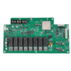
Diseñamos esta PCBA de PCB de 2 caras específicamente para aplicaciones de conectividad de impresoras., integrando circuito impreso flexible (FPC) capacidades de programación de circuitos integrados y tecnología.
Diseñado para una comunicación perfecta entre sistemas de impresión, Esta PCB FR4 de 1,6 mm se adapta a todo, desde impresoras domésticas hasta máquinas industriales.. Ofrece un fuerte soporte mecánico y un rendimiento eléctrico estable., garantizando un funcionamiento fiable en entornos exigentes.
Optimizamos la arquitectura de dos caras de PCBA para un enrutamiento de señal eficiente y una integración perfecta de componentes..
- Estructura de capas: La PCB FR4 de doble cara (Tg130°C) admite montaje mixto, con componentes SMT (como MCU y controladores IC) colocado en la capa superior y componentes THT (incluidos conectores de alimentación y enchufes FPC) en la capa inferior. El 1OZ (35μm) El espesor del cobre garantiza una transmisión de corriente estable., Manejo de hasta 3 A para componentes que consumen mucha energía..
- Integración FPC: Equipado con conectores FFC/FPC de paso de 0,5 mm (P.EJ., Serie JAE LY), La PCBA admite interfaces de 50 a 100 pines con un radio de curvatura de ≥5 mm., capaz de soportar más 10,000 ciclos flexibles. La flexibilidad permite un cableado confiable para mover piezas de impresora en espacios limitados.
- Programación IC: Con programación en el sistema (ISP) e interfaces de depuración JTAG/SWD, La PCBA permite la actualización previa del firmware., incluidos algoritmos de control de impresión y protocolos de comunicación. Admite actualizaciones USB y compatibilidad con MCU para funciones de impresora personalizadas.
La PCBA se somete a un meticuloso proceso de ensamblaje para garantizar precisión y confiabilidad.:
Imprimir Pegar y SPI:
Utilice soldadura en pasta SAC305 sin plomo con una plantilla cortada con láser de 0,12 mm.. 3D SPI garantiza la precisión del volumen de pasta dentro 5%, Prevención de cortocircuitos en circuitos integrados de paso fino. (0.5paso mm).
Elegir & Colocar y refluir:
Pick-and-place de alta precisión (±25μm) lugares 0402 componentes. El reflujo de nitrógeno a 255 °C reduce la oxidación y garantiza uniones de soldadura confiables.
AOI y THT:
La inspección óptica automatizada detecta errores de desalineación y polaridad antes de soldar por ola piezas THT a 250°C. Las juntas pasan una prueba de fuerza de tracción de 3N.
Pruebas funcionales y cumplimiento:
Las pruebas eléctricas verifican la integridad de la señal. (≥10Mbps), onda de poder (≤50mV), y compatibilidad de protocolos (USB 2.0, UART).
Los rayos X escanean los circuitos integrados BGA para mantener los huecos debajo 10%.
Las pruebas ambientales incluyen 300 ciclos térmicos (-20°C a 60°C) y 96 horas de calor humedo (40°C/93% HR).
- Impresoras domésticas: Ideal para placas base de impresoras láser y de inyección de tinta, PCBA permite la transferencia de datos de alta velocidad para el procesamiento de imágenes y el posicionamiento preciso del cabezal de impresión a través de conexiones FPC.
- Impresoras de etiquetas industriales: Diseñado para soportar vibraciones en líneas de producción., admite la generación de códigos de barras y códigos QR a través de programación IC personalizada, asegurando una impresión de etiquetas precisa y consistente.
- Impresoras Térmicas: Utilizado en sistemas POS y dispositivos médicos., Soporta protocolos de comunicación USB/serie.. Los circuitos integrados preprogramados agilizan la integración, Reducir el tiempo de desarrollo para los clientes..
- Solución integral: Ofreciendo servicios integrales desde la fabricación de PCB. (línea mínima/espacio: 100μm), abastecimiento de componentes (distribuidores autorizados para TI, CALLE, Murata), Montaje SMT/THT, Programación IC, a pruebas funcionales.
- Personalización de FPC: Adapta los FPC a requisitos específicos, incluyendo espesor (0.1-0.3mm), adaptación de impedancia (50Ω/75Ω), capas de blindaje (lámina de aluminio/cobre), y acabados superficiales (chapado en oro/niquelado).
- Respuesta Rápida: Plazo de entrega estándar de 4-5 semanas; Fai (Inspección del primer artículo) informes y trazabilidad completa del material (Cumple con RoHS/REACH) se proporcionan. Ensayos en lotes pequeños (100-500 unidades) puede acelerarse dentro de 2 semanas.
PCBA personalizada de 2 caras con programación FPC e IC para estabilidad, conectividad de impresora flexible. Ya sea para aplicaciones industriales o de consumo, establece un estándar para la conectividad, flexibilidad, y fiabilidad en la tecnología de impresión.