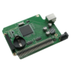
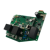
This 2-layer FR4 PCB addresses the needs of industrial automation, sensor networks, and power management applications requiring a balance of compact design and robust performance. With dimensions of 100×79.69mm and a 1.6mm thickness, the board offers a versatile platform for integrating microcontrollers, communication interfaces, and power components in a space-efficient form factor. Constructed from FR4 material, it ensures stable electrical insulation (dielectric constant εr=4.5) and mechanical rigidity, suitable for operation in moderate-temperature industrial environments with minimal vibration.
- 2-Layer Stackup:
- Top and bottom signal layers with ground/power planes implemented via copper pours, reducing electromagnetic interference (EMI) for basic signal integrity.
- Split power domains (e.g., 5V/3.3V) separated by isolation traces to minimize cross-talk between analog and digital sections.
- 1OZ (35μm) Copper Thickness:
- Supports up to 8A current in power traces (≥1mm width) for motor drivers or solenoid valves.
- Enables fine-line routing (minimum line/space: 100μm/100μm) for low-speed signals (UART, I2C) and component density.
- Green LPI Solder Mask:
- Standard industrial color for easy visual inspection during assembly and maintenance.
- Chemical resistance against oils, coolants, and cleaning agents common in manufacturing environments.
- ENIG Surface Finish:
- 3–5μm nickel layer for corrosion protection; 0.05–0.1μm gold layer ensures reliable solderability for both SMT and DIP components, even after long-term storage.
- SMT+DIP Mixed Assembly:
- SMT: Accommodates 0402 passive components, SOIC/SSOP ICs, and 0.5mm pitch QFP packages for high-density integration.
- DIP: Supports through-hole connectors (e.g., 0.1″ headers, terminal blocks) and relays for robust field wiring in industrial setups.
- Precision Fabrication:
- Laser direct imaging (LDI) for 100μm trace accuracy, ensuring consistent routing across the board.
- Electrolytic copper plating with uniform thickness verification to maintain conductivity.
- Comprehensive Testing:
- 100% automated optical inspection (AOI) to verify solder mask coverage and silkscreen clarity.
- Flying probe testing for electrical continuity (≤0.1Ω) and isolation (≥100MΩ) to eliminate open/short circuits.
- Thermal stress testing (260°C reflow cycles) to ensure solder joint reliability during assembly.
- Standards Compliance:
- Meets IPC-6012 Class 2 standards for industrial electronics.
- RoHS/REACH compliant for lead-free and hazardous substance restrictions.
- Industrial Sensor Modules:
Integrates temperature, humidity, or pressure sensors with analog signal conditioning and wireless communication (e.g., LoRa, BLE).
- Motor Control Units:
Drives low-voltage DC motors in conveyor systems, featuring PWM control, current limiting, and overheat protection.
- Communication Interfaces:
Enables protocol conversion (e.g., RS-485 to USB) for legacy industrial equipment integration with modern control systems.
- Power Distribution Panels:
Manages 24V DC power distribution to multiple loads, with circuit protection (fuses, TVS diodes) and status indication LEDs.