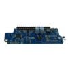
This 8-layer FR4 PCB addresses the challenges of high-density, narrow-format electronic designs, where space efficiency and signal integrity are critical. Với kích thước của 165.50×25.90mm và một 1.6độ dày mm, the board provides a compact yet robust platform for integrating complex circuitry in applications such as industrial sensors, communication modules, and portable test equipment. Xây dựng từ vật liệu FR4, nó cung cấp cách điện ổn định (Hằng số điện môi εr = 4,5) và độ bền cơ học, thích hợp để hoạt động trong môi trường có nhiệt độ và độ rung vừa phải.
- 8-Xếp chồng lớp:
- 4 Lớp tín hiệu + 4 mặt phẳng nguồn/mặt đất để triệt tiêu EMI hiệu quả
- Alternating signal and power planes minimize cross-talk and impedance variations
- 1Oz (35μm) Độ dày đồng:
- Balances fine-line routing (dòng/khoảng trắng tối thiểu: 75μm/75μm) with current-carrying capacity (up to 8A per trace)
- Kiểm soát trở kháng chính xác:
- 50Ω ±8% đối với cấu hình microstrip/stripline
- Critical for maintaining signal integrity in high-speed interfaces (ví dụ., USB 3.0, CAN FD)
- Mặt nạ hàn LPI màu xanh:
- Distinctive color for easy visual inspection in narrow layouts
- Chemical resistance against industrial contaminants
- Bề mặt hoàn thiện ENIG:
- 3–5μm lớp niken để chống ăn mòn
- 0.05–Lớp vàng 0,1μm cho khả năng hàn lâu dài và khả năng tương thích liên kết dây
- Mixed SMT+DIP Assembly:
- SMT support for high-density ICs (ví dụ., microcontrollers, FPGA)
- DIP compatibility for rugged connectors (ví dụ., 0.1” tiêu đề, khối thiết bị đầu cuối) and through-hole components
- Chế tạo có độ chính xác cao:
- Hình ảnh trực tiếp bằng laser (LDI) cho độ chính xác theo dõi 75μm
- Electrolytic copper plating with ±5% thickness uniformity
- Kiểm tra toàn diện:
- 100% AOI inspection for solder mask and silkscreen quality
- X-ray verification of BGA vias
- Thử nghiệm đầu dò bay để xác định tính liên tục và cách ly điện
- Tuân thủ môi trường:
- Lớp IPC-6012 2 for industrial applications
- Tuân thủ RoHS/REACH để hạn chế chất độc hại
- Thermal cycling tested (-40° C đến +85 ° C., 500 chu kỳ)
- Mô-đun cảm biến công nghiệp:
Supports high-density sensor interfaces, signal conditioning, và các giao thức truyền thông (ví dụ., Modbus, Profibus) in a narrow form factor.
- Communication Gateways:
Enables multi-protocol conversion (ví dụ., Ethernet to RS-485) with compact PCB real estate.
- Portable Test Equipment:
Integrates measurement circuitry and user interfaces in handheld devices.
- Automotive Control Units:
Fits into space-constrained compartments while maintaining signal integrity in harsh environments.
By integrating 8-layer signal isolation, 1OZ copper conductivity, và độ bền ENIG, this PCB delivers uncompromised performance in demanding, space-constrained applications. The blue solder mask offers visual distinction in complex layouts, while mixed SMT/DIP assembly supports both high-density digital components and robust field connections. Được hỗ trợ bởi ISO 9001:2015 chứng nhận, it provides the foundation for reliable, compact electronic systems requiring both performance and durability.