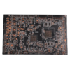
This 6-layer FR4 TG170 PCB delivers high performance for industrial automation, 5G communication modules, and other mission-critical electronics. Featuring a 1.6mm thickness, 1OZ copper on all layers, and an ENIG surface finish, it balances thermal stability, Tính toàn vẹn tín hiệu, and mechanical durability effectively.
Because it uses FR4 material with a Tg of 170°C, this PCB withstands harsh industrial environments like factory floors, outdoor communication hubs, and automotive systems. Its 6-layer design includes 4 lớp tín hiệu và 2 Máy bay điện/mặt đất, which actively reduce electromagnetic interference (Emi). Vì thế, it ensures stable data transmission in applications such as PLCs, industrial IoT gateways, and wireless base stations.
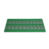
A key feature is the gold finger with 2 microinch plating, which provides excellent corrosion resistance and durable electrical contacts. This design suits systems requiring frequent board insertion/removal, including modular industrial systems and rack-mounted communication devices. Furthermore, the ENIG finish enhances solderability and wire bonding. It uses a nickel barrier to prevent oxidation and a thin gold layer optimized for fine-pitch components.
We apply a strict fabrication process to ensure precision and consistency:
Inner Layer Processing: Hình ảnh trực tiếp bằng laser (LDI) defines fine 75μm traces on 1OZ copper.
khoan & mạ: Precision mechanical drilling and plated-through holes (PTH) ensure robust electrical vias.
Outer Layer Patterning: Dry film lamination and tin plating protect circuitry during etching.
Hoàn thiện bề mặt: The ENIG coating combined with a green LPI solder mask enhances durability and visual clarity.
Kiểm soát chất lượng: We perform 100% thử nghiệm điện (Kiểm tra điện tử) and automated optical inspection (Aoi) to guarantee defect-free boards. We strictly reject any X-out panels to maintain high quality.
Industrial Control Systems: Provide reliable power and signal integrity for PLCs and motor drives.
5G & Truyền thông không dây: Support RF integrity in 5G sub-6GHz and Wi-Fi 6 thiết bị.
Thiết bị y tế: Comply with RoHS/REACH and biocompatibility standards.
Không gian vũ trụ & Phòng thủ: Resist vibration and temperature cycling in rugged environments.
Ổn định nhiệt: It outperforms standard FR4 and reduces delamination risk.
Reliable Gold Finger Contacts: Ensure low resistance and long-lasting performance.
Thiết kế linh hoạt: Support mixed SMT/DIP assembly with fine-pitch compatibility.
Global Compliance: Meet IPC-6012 Class 2 quality standards for consistent mass production.
Engineers developing smart factory automation, telecommunications infrastructure, or high-reliability medical electronics will find this PCB offers performance, scalability, and certification needed for next-generation industrial and communication technologies.