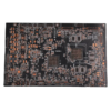
This 6-layer FR4 TG170 PCB is a high-performance printed circuit board engineered for industrial automation, communication modules, and mission-critical electronic systems that demand superior thermal stability, sinyal bütünlüğü, and mechanical durability. With a 1.6mm thickness, 1OZ copper on all layers, and an ENIG surface finish, the board balances robust power handling with fine-pitch routing capabilities, making it ideal for applications ranging from industrial control panels to 5G communication devices and medical equipment.


Constructed from FR4 material with a glass transition temperature (Tg) of 170°C, the PCB withstands prolonged exposure to elevated temperatures in harsh industrial environments, such as factory floors, outdoor communication hubs, or automotive systems. The 6-layer architecture—featuring 4 signal layers and 2 dedicated power/ground planes—minimizes electromagnetic interference (EMI) and enables efficient separation of high-speed signals (Örn., Ethernet, CANbus) from power circuits. This design ensures stable signal transmission for applications requiring real-time data processing, such as programmable logic controllers (PLCs), industrial IoT gateways, or wireless base stations.


A key feature of this PCB is the gold finger with a 2 microinch (0.05μm) altın kalınlığı, providing exceptional corrosion resistance and reliable electrical contact in pluggable connectors. The gold plating enhances wear resistance during mating cycles, making it suitable for applications requiring frequent board insertion/removal, such as modular industrial systems or rack-mounted communication equipment. The ENIG (Elektroles Nikel Daldırma Altın) surface finish further ensures long-term solderability and wire bonding compatibility, with a 3-5μm nickel barrier layer preventing copper oxidation and a thin gold layer optimizing soldering precision for fine-pitch components (down to 0.5mm pitch).

Manufacturing Process & Kalite güvencesi

The PCB undergoes a rigorous fabrication process to ensure precision and reliability:


  1. Inner Layer Processing: Laser direct imaging (LDI) defines 75μm line/space patterns on 1OZ copper cores, followed by etching to form the inner circuitry.
  2. Drilling & Plating: High-precision mechanical drilling creates vias, which are then processed through PTH (plated through hole) with electroless and electrolytic copper plating to achieve uniform 35μm thickness, ensuring robust through-hole conductivity.
  3. Outer Layer Pattern Transfer: Dry film lamination and exposure define the outer layer traces, followed by pattern plating and tin masking to protect conductive areas during etching.
  4. Surface Finishing: The ENIG process applies a consistent nickel-gold coating, while the green LPI solder mask provides chemical resistance and visual clarity for component identification.
  5. E-Test & Kalite kontrolü: 100% electrical testing verifies continuity (≤0.1Ω) and isolation (≥100MΩ), while automated optical inspection (AOI) ensures solder mask coverage and gold finger integrity. Notably, X-out panels are strictly rejected during quality checks to eliminate defective boards from production.

Applications & Advantages

  • Industrial Control Systems: Supports PLCs and motor drives with stable power distribution and high-speed signal routing for real-time control.
  • 5G & Wireless Communication: Enables RF signal integrity in 5G sub-6GHz modules and Wi-Fi 6 access points, thanks to controlled impedance (50Ω ±8%) and layer stackup optimization.
  • Medical Devices: Meets biocompatibility requirements for diagnostic equipment, with lead-free compliance (RoHS/REACH) and low outgassing materials.
  • Aerospace & Defense: Withstands vibration and temperature cycling (-40°C to +85°C) in avionics and ruggedized electronic systems.


The PCB’s TG170 material, 6-katman mimarisi, and gold finger design collectively offer:


  • Thermal Stability: Reduces delamination risks in high-temperature environments compared to standard FR4 (Tg130°C).
  • Reliable Interconnects: Gold fingers ensure low contact resistance and long service life in dynamic mating applications.
  • Design Flexibility: Supports mixed technology assembly (SMT/DIP) and accommodates components from 0402 passives to QFP/BGA packages.


Compliant with IPC-6012 Class 2 standartlar, this 6-layer FR4 TG170 PCB delivers consistent quality for mid-to-high-volume production. Its combination of thermal performance, sinyal bütünlüğü, and robust mechanical design makes it a strategic choice for engineers developing next-generation industrial and communication systems that require reliability, scalability, and compliance with global standards. Whether used in smart factory automation, telecommunications infrastructure, or advanced medical devices, this PCB provides the foundation for innovative, high-performance electronics.

PCB özelliği


Öğe Standart PCB Özelleştirilmiş PCB
Katman sayısı 2-20 2-50
Malzeme Fr4 Merhaba Tayvan Birliği'nden Hızlı Malzeme, Ve teknoloji, Rogers vb..
PCB kalınlığı 0.4-3.2mm 0.4-6.4mm
Bakır ağırlığı Getir-3o Getir-10
Min. Delik 0.3mm 0.1Lazer Matkap tarafından MM
PCB Boyutu Min. 6.00X6.00mm maks.. 600.00X620.00mm
PCB Finish Hall, Hal-Leadfree, Kabul etmek, Enepik, Daldırma tenekesi, Dalma gümüşü, Osp
Min.SoldMask Barajı. 41 oz için Mils 2.51 oz için Mils
Hazırlık türü 2116,1080 2116,1080,7628,3313,106
Min.Width/Alan 4/4 Mils 2.5/2.5 Mils
Min. Halka halka 4/4 Mils 2.5/2.5 Mils
En boy oranı 8:1 15:1
Kurşun zamanı 2 haftalar 5 Günler - 5 Haftalar
Empedans toleransı ±5% - ±10% ±5% - ±10%
Diğer teknikler Altın parmaklar, Kör ve gömülü delikler, Soyulabilir lehim maskesi, Kenar kaplama, Karbon maskesi, Holestersink Deliği,
Yarım/Castellated Delik, Basın Deliği, Takılı/reçine ile doldurulmuş, Pad'de (vip, POFV), Bir PCB'de Çoklu Bitli

Bu kapanacak 0 saniye

PCBA yeteneği


HAYIR. Öğe Proses Yeteneği parametresi
1 Sipariş miktarı 1 adetten fazla
2 PCB Türü Rijit PCB, FPC, Katı fleks pcb
3 Montaj teknolojisi SMT, Tht, Karışık teknoloji veya pop
4 Bileşen kaynak Tam anahtar teslim, Kısmi anahtar teslim, Sevk edilmiş
5 PCB Boyutu 45*45mm -- 510*500mm
6 BGA paketi BGA onu. 0.14mm, BGA 0.2mm perde
7 Parça Sunumu Kaset, Makara, Sopa veya tepsiye
8 Tel & Kablo Tel kablo demeti ve kablo düzeneği
9 Kalite denetimi Görsel, SPI, Fai, AOI; X-ışını kontrolü
10 Montaj doğruluğu ±0.035mm (±0.025mm)
11 Min Paket 01005 (0.4mm*0.2mm)
12 Konformal kaplama Makine tarafından kullanılabilir
13 İc denetimi İşlev, Elektrik veya Decap Testi
14 Kurşun zamanı 3 günler - 5 Haftalar
15 Diğer teknikler Kutu Yapı Montajı, IC programlama, Bileşenler Maliyet Aşağı, İşlev & Özel olarak yaşlanma testi,
Basın montajı, SAC305 veya daha iyi lehim macunu kullanılan, BGA Reballing veya Repwork,
EMI emisyon kontrolü için kalkan örtü montajı

Bu kapanacak 0 saniye

FPC yeteneği


HAYIR. Öğe Proses Yeteneği parametresi
1 Katman sayısı 1-8 Katmanlar
2 FPC malzemesi Pi, Evcil hayvan, DOLMA KALEM, FR-4
3 Son kalınlık 0.06-4.0mm
4 Tahta boyutu 250.00X1200mm
5 Bakır folyo 12bir,18bir,35bir,70bir
6 Min genişlik/boşluk 3bin/3mil
7 Holewall bakır kalınlığı 8-20μm
8 Yüzey tedavisi Salon Leaddree, Kabul etmek, Daldırma gümüş/kalay, Osp
9 Boyutu özetler ± 2mils
10 Lehim ısı direnci 280℃ / 10snats
11 Sertleştirici Türü Pi, Fr4, Paslanmaz çelik, Alüminyum
12 Min. Delik Günü (Pth) 0.1mm ± 3mils
13 Min. Delik Günü (Npth) 0.25± 2mils
14 Maksimum/dk Soldmask kalınlığı 2MIL/0.5mil (50bir/12.7um)
15 Min Yuvası 0.8mm × 1mm

Bu kapanacak 0 saniye