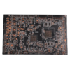
This 6-layer FR4 TG170 PCB is a high-performance printed circuit board engineered for industrial automation, communication modules, and mission-critical electronic systems that demand superior thermal stability, целостность сигнала, and mechanical durability. With a 1.6mm thickness, 1OZ copper on all layers, and an ENIG surface finish, the board balances robust power handling with fine-pitch routing capabilities, making it ideal for applications ranging from industrial control panels to 5G communication devices and medical equipment.


Constructed from FR4 material with a glass transition temperature (Tg) of 170°C, the PCB withstands prolonged exposure to elevated temperatures in harsh industrial environments, such as factory floors, outdoor communication hubs, or automotive systems. The 6-layer architecture—featuring 4 signal layers and 2 dedicated power/ground planes—minimizes electromagnetic interference (Эми) and enables efficient separation of high-speed signals (НАПРИМЕР., Ethernet, CANbus) from power circuits. This design ensures stable signal transmission for applications requiring real-time data processing, such as programmable logic controllers (PLCs), industrial IoT gateways, or wireless base stations.


A key feature of this PCB is the gold finger with a 2 microinch (0.05мкм) толщина золота, providing exceptional corrosion resistance and reliable electrical contact in pluggable connectors. The gold plating enhances wear resistance during mating cycles, making it suitable for applications requiring frequent board insertion/removal, such as modular industrial systems or rack-mounted communication equipment. The ENIG (Электролетное никелевое погружение) surface finish further ensures long-term solderability and wire bonding compatibility, with a 3-5μm nickel barrier layer preventing copper oxidation and a thin gold layer optimizing soldering precision for fine-pitch components (down to 0.5mm pitch).

Manufacturing Process & Гарантия качества

The PCB undergoes a rigorous fabrication process to ensure precision and reliability:


  1. Inner Layer Processing: Laser direct imaging (LDI) defines 75μm line/space patterns on 1OZ copper cores, followed by etching to form the inner circuitry.
  2. Drilling & Plating: High-precision mechanical drilling creates vias, which are then processed through PTH (plated through hole) with electroless and electrolytic copper plating to achieve uniform 35μm thickness, ensuring robust through-hole conductivity.
  3. Outer Layer Pattern Transfer: Dry film lamination and exposure define the outer layer traces, followed by pattern plating and tin masking to protect conductive areas during etching.
  4. Surface Finishing: The ENIG process applies a consistent nickel-gold coating, while the green LPI solder mask provides chemical resistance and visual clarity for component identification.
  5. E-Test & Контроль качества: 100% electrical testing verifies continuity (≤0.1Ω) and isolation (≥100MΩ), while automated optical inspection (Аои) ensures solder mask coverage and gold finger integrity. Notably, X-out panels are strictly rejected during quality checks to eliminate defective boards from production.

Applications & Advantages

  • Industrial Control Systems: Supports PLCs and motor drives with stable power distribution and high-speed signal routing for real-time control.
  • 5G & Wireless Communication: Enables RF signal integrity in 5G sub-6GHz modules and Wi-Fi 6 access points, thanks to controlled impedance (50Ω ±8%) and layer stackup optimization.
  • Medical Devices: Meets biocompatibility requirements for diagnostic equipment, with lead-free compliance (RoHS/REACH) and low outgassing materials.
  • Aerospace & Defense: Withstands vibration and temperature cycling (-40° C до +85 ° C.) in avionics and ruggedized electronic systems.


The PCB’s TG170 material, 6-архитектура слоя, and gold finger design collectively offer:


  • Thermal Stability: Reduces delamination risks in high-temperature environments compared to standard FR4 (Tg130°C).
  • Reliable Interconnects: Gold fingers ensure low contact resistance and long service life in dynamic mating applications.
  • Design Flexibility: Supports mixed technology assembly (SMT/DIP) and accommodates components from 0402 passives to QFP/BGA packages.


Compliant with IPC-6012 Class 2 стандарты, this 6-layer FR4 TG170 PCB delivers consistent quality for mid-to-high-volume production. Its combination of thermal performance, целостность сигнала, and robust mechanical design makes it a strategic choice for engineers developing next-generation industrial and communication systems that require reliability, scalability, and compliance with global standards. Whether used in smart factory automation, telecommunications infrastructure, or advanced medical devices, this PCB provides the foundation for innovative, high-performance electronics.

Возможность печатной платы


Элемент Стандартная печатная плата Индивидуальная печатная плата
Количество слоев 2-20 2-50
Материал FR4 Hi Speed ​​Material от Taiwan Union, И технология, Высокочастотный материал от Роджерса и т. Д..
Толщина печатной платы 0.4-3.2мм 0.4-6.4мм
Медный вес Принесите-3o Принесите 10
Мин. Диаметр отверстия 0.3мм 0.1мм от лазерной тренировки
Размер печатной платы Мин. 6.00X6.00 мм макс. 600.00X620,00 мм
Печата финиш Отстранение, Hal-Leadfree, Соглашаться, Enepic, Погружение, Погружение серебро, Оп
Мин. 4мил за 1 унцию 2.5мил за 1 унцию
Тип преорета 2116,1080 2116,1080,7628,3313,106
Min.width/пространство 4/4 мил 2.5/2.5 мил
Мин. Кольцевое кольцо 4/4 мил 2.5/2.5 мил
Соотношение сторон 8:1 15:1
Время выполнения 2 недели 5 Дни - 5 Недели
Импеданс терпимость ±5% - ±10% ±5% - ±10%
Другие методы Золотые пальцы, Слепые и похороненные отверстия, Отчитываемая паяная маска, Кравление, Углеродная маска, HOLERSICK HOLE,
Половина/Кастелленная дыра, Нажмите отверстие для подключения, Через подключенную/заполненную смолой, Через Pad (VIP, Пофв), Многофинансы на одной печатной плате

Он будет закрыт в 0 секунд

Возможность PCBA


Нет. Элемент Параметр возможностей процесса
1 Количество заказа Более 1 шт
2 Тип печатной платы Жесткая печатная плата, FPC, Жесткая пласка
3 Ассамблея Пост, Это, Смешанная технология или поп
4 Компонентный источник Полный под ключ, Частичный под ключ, Отправлено
5 Размер печатной платы 45*45мм -- 510*500мм
6 BGA Package BGA ее. 0.14мм, BGA 0,2 мм шаг
7 Презентация деталей Лента, Катушка, Палка или поднос
8 Проволока & Кабель Проволочная жгут и кабельная сборка
9 Качественная проверка Визуальный, SPI, Фей, Аои; Рентгеновская проверка
10 Точность монтажа ±0.035мм (±0.025мм)
11 Мин пакет 01005 (0.4мм*0,2 мм)
12 Конформное покрытие Доступно на машине
13 IC Inspection Функция, Электрический тест или DECAP
14 Время выполнения 3 дни - 5 Недели
15 Другие методы Сборка коробки сборка, IC программирование, Компоненты стоимость, Функция & Испытание на старение как пользовательский,
Нажмите Fit Assembly, SAC305 или лучшая паяная паста используется, BGA REBALLING или REWORD,
Узел крышки щита для контроля эмиссии EMI

Он будет закрыт в 0 секунд

Возможность FPC


Нет. Элемент Параметр возможностей процесса
1 Количество слоев 1-8 Слои
2 Материал FPC Пик, ДОМАШНИЙ ПИТОМЕЦ, РУЧКА, FR-4
3 Окончательная толщина 0.06-4.0мм
4 Размер доски 250.00X1200 мм
5 Медная фольга 12один,18один,35один,70один
6 Мин ширина/пространство 3тысяча/3 мили
7 HOLEWALL CODINGE 8-20мкм
8 Поверхностная обработка Холл Лидерри, Соглашаться, Погружение серебро/олово, Оп
9 Определяет измерение ± 2 мили
10 Припаяя теплостойкость 280℃ / 10секунды
11 Тип жесткости Пик, FR4, Нержавеющая сталь, Алюминий
12 Мин. День дыры (Пт) 0.1мм ± 3 мили
13 Мин. День дыры (Npth) 0.25± 2 мили
14 Макс/мин толщины солдата 2Мил/0,5 млн (50Один/12,7 мм)
15 Мин слот 0.8мм × 1 мм

Он будет закрыт в 0 секунд