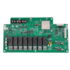
This 2-sided PCB PCBA is a purpose-built solution tailored for printer connectivity applications, integrating Flexible Printed Circuit (FPC) technology and IC programming capabilities. Designed to facilitate seamless communication between printer components, control units, and user interfaces, it meets the demands of modern printing devices, from compact home printers to industrial-grade label printers and multifunctional office equipment. The 1.6mm-thick FR4 PCB provides a robust foundation, balancing mechanical strength with excellent electrical performance, ensuring reliable operation even in dynamic and high-frequency environments.

Core Design and Connectivity Advantages

The PCBA’s 2-sided architecture is optimized for efficient signal routing and component integration:


  • Layer Structure: The double-sided FR4 PCB (Tg130°C) supports mixed assembly, with SMT components (such as MCUs and driver ICs) placed on the top layer and THT components (including power connectors and FPC sockets) on the bottom layer. The 1OZ (35мкм) copper thickness ensures stable current transmission, handling up to 3A for power-hungry components.
  • FPC Integration: Equipped with 0.5mm pitch FFC/FPC connectors (НАПРИМЕР., JAE LY series), the PCBA supports 50-100-pin interfaces with a bend radius of ≥5mm, capable of withstanding over 10,000 flex cycles. This flexibility is crucial for connecting dynamic printer parts, such as printheads, which require reliable yet adaptable wiring in confined spaces.
  • IC программирование: Featuring in-system programming (ISP) and JTAG/SWD debug interfaces, the PCBA allows for pre-flashing of firmware, including print control algorithms and communication protocols. It also supports on-site updates via USB, compatible with popular MCU platforms like STM32 and ESP32, enabling customization to meet specific printer functions.

Manufacturing Process and Quality Control

The PCBA undergoes a meticulous assembly process to ensure precision and reliability:


  1. Print Paste and SPI:
    • Lead-free solder paste (SAC305) is applied using a laser-cut stencil (0.12ММ толщина), and 3D Solder Paste Inspection (SPI) verifies paste volume with <5% variance, preventing bridging on fine-pitch components like QFP/QFN ICs (0.5mm pin pitch).
  2. Выбирать & Place and Reflow:
    • High-precision pick-and-place machines (±25μm repeatability) position 0402 components and ICs, followed by nitrogen reflow soldering at 255°C to reduce oxidation and ensure high-quality joints on delicate pins.
  3. AOI and THT Processes:
    • Автоматическая оптическая проверка (Аои) detects component misalignment and polarity errors before THT components, such as FPC sockets and power connectors, undergo wave soldering at 250°C. The soldered joints meet a minimum pull force of 3N for reliability.
  4. Functional Testing and Compliance:
    • Electrical Performance: Tests verify signal integrity on FPC interfaces (transmission speeds ≥10Mbps), power ripple (≤50mV), and compatibility with communication protocols (НАПРИМЕР., USB 2.0, UART).
    • Рентгеновский осмотр: BGA-packaged ICs (НАПРИМЕР., print control chips) are scanned with X-ray tomography to ensure void rates within 10%.
    • Environmental Testing: The PCBA endures 300 thermal cycles (-20°C to +60°C) и 96 hours of damp heat testing (40°C/93%RH) to validate performance in harsh conditions.

Applications and Customization Capabilities

  • Home Printers: Ideal for inkjet and laser printer mainboards, the PCBA enables high-speed data transfer for image processing and precise printhead positioning via FPC connections.
  • Industrial Label Printers: Designed to withstand vibrations on production lines, it supports barcode and QR code generation through custom IC programming, ensuring accurate and consistent label printing.
  • Thermal Printers: Used in POS systems and medical devices, it supports USB/serial communication protocols. Pre-programmed ICs streamline integration, reducing development time for customers.

Differentiated Advantages and Services

  • One-Stop Solution: Offering comprehensive services from PCB fabrication (minimum line/space: 100мкм), component sourcing (authorized distributors for TI, ST, Murata), SMT/THT assembly, IC программирование, to functional testing.
  • FPC Customization: Tailors FPCs to specific requirements, including thickness (0.1-0.3мм), impedance matching (50Ω/75Ω), shielding layers (aluminum/copper foil), and surface finishes (gold/nickel plating).
  • Rapid Response: Standard lead time of 4-5 недели; Фей (Первая статья проверка) reports and full material traceability (RoHS/REACH compliant) are provided. Small-batch trials (100-500 units) can be expedited within 2 недели.


This PCBA for printer connectivity, featuring FPC integration and IC programming on a 2-sided PCB, guarantees reliable signal transmission and customizable functionality. Its precision manufacturing, combined with stringent quality control, makes it an ideal choice for OEMs aiming to enhance printer performance and streamline development cycles. Whether for consumer or industrial applications, it sets a standard for connectivity, flexibility, and reliability in printing technology.

Возможность печатной платы


Элемент Стандартная печатная плата Индивидуальная печатная плата
Количество слоев 2-20 2-50
Материал FR4 Hi Speed ​​Material от Taiwan Union, И технология, Высокочастотный материал от Роджерса и т. Д..
Толщина печатной платы 0.4-3.2мм 0.4-6.4мм
Медный вес Принесите-3o Принесите 10
Мин. Диаметр отверстия 0.3мм 0.1мм от лазерной тренировки
Размер печатной платы Мин. 6.00X6.00 мм макс. 600.00X620,00 мм
Печата финиш Отстранение, Hal-Leadfree, Соглашаться, Enepic, Погружение, Погружение серебро, Оп
Мин. 4мил за 1 унцию 2.5мил за 1 унцию
Тип преорета 2116,1080 2116,1080,7628,3313,106
Min.width/пространство 4/4 мил 2.5/2.5 мил
Мин. Кольцевое кольцо 4/4 мил 2.5/2.5 мил
Соотношение сторон 8:1 15:1
Время выполнения 2 недели 5 Дни - 5 Недели
Импеданс терпимость ±5% - ±10% ±5% - ±10%
Другие методы Золотые пальцы, Слепые и похороненные отверстия, Отчитываемая паяная маска, Кравление, Углеродная маска, HOLERSICK HOLE,
Половина/Кастелленная дыра, Нажмите отверстие для подключения, Через подключенную/заполненную смолой, Через Pad (VIP, Пофв), Многофинансы на одной печатной плате

Он будет закрыт в 0 секунд

Возможность PCBA


Нет. Элемент Параметр возможностей процесса
1 Количество заказа Более 1 шт
2 Тип печатной платы Жесткая печатная плата, FPC, Жесткая пласка
3 Ассамблея Пост, Это, Смешанная технология или поп
4 Компонентный источник Полный под ключ, Частичный под ключ, Отправлено
5 Размер печатной платы 45*45мм -- 510*500мм
6 BGA Package BGA ее. 0.14мм, BGA 0,2 мм шаг
7 Презентация деталей Лента, Катушка, Палка или поднос
8 Проволока & Кабель Проволочная жгут и кабельная сборка
9 Качественная проверка Визуальный, SPI, Фей, Аои; Рентгеновская проверка
10 Точность монтажа ±0.035мм (±0.025мм)
11 Мин пакет 01005 (0.4мм*0,2 мм)
12 Конформное покрытие Доступно на машине
13 IC Inspection Функция, Электрический тест или DECAP
14 Время выполнения 3 дни - 5 Недели
15 Другие методы Сборка коробки сборка, IC программирование, Компоненты стоимость, Функция & Испытание на старение как пользовательский,
Нажмите Fit Assembly, SAC305 или лучшая паяная паста используется, BGA REBALLING или REWORD,
Узел крышки щита для контроля эмиссии EMI

Он будет закрыт в 0 секунд

Возможность FPC


Нет. Элемент Параметр возможностей процесса
1 Количество слоев 1-8 Слои
2 Материал FPC Пик, ДОМАШНИЙ ПИТОМЕЦ, РУЧКА, FR-4
3 Окончательная толщина 0.06-4.0мм
4 Размер доски 250.00X1200 мм
5 Медная фольга 12один,18один,35один,70один
6 Мин ширина/пространство 3тысяча/3 мили
7 HOLEWALL CODINGE 8-20мкм
8 Поверхностная обработка Холл Лидерри, Соглашаться, Погружение серебро/олово, Оп
9 Определяет измерение ± 2 мили
10 Припаяя теплостойкость 280℃ / 10секунды
11 Тип жесткости Пик, FR4, Нержавеющая сталь, Алюминий
12 Мин. День дыры (Пт) 0.1мм ± 3 мили
13 Мин. День дыры (Npth) 0.25± 2 мили
14 Макс/мин толщины солдата 2Мил/0,5 млн (50Один/12,7 мм)
15 Мин слот 0.8мм × 1 мм

Он будет закрыт в 0 секунд