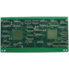
10-Печатная плата FR4 с контролем импеданса слоя разработана для высокоскоростных электронных систем, требующих точной целостности сигнала, например, центры обработки данных, сетевое оборудование, и современные устройства связи. Многослойная структура объединяет 10 слои подложки FR4 (1.6мм общая толщина) для обеспечения сложной маршрутизации для цепей с высокой плотностью, Пока BGA (Шариковая сетка массив) с заглушенными переходными отверстиями обеспечивает надежные соединения для критически важных компонентов. А 50Ом±8% контроль импеданса минимизирует отражение сигнала и перекрестные помехи, что делает его идеальным для высокочастотных приложений, таких как PCIe 4.0, USB 3.2, или системы Ethernet.
А Соглашаться (Электролетное никелевое погружение) обработка поверхности обеспечивает гладкость, устойчивое к окислению покрытие, улучшение паяемости и долговременной надежности. Материал FR4 обеспечивает баланс экономичности и электрической стабильности. (Диэлектрическая постоянная εr = 4,5), подходит как для коммерческого, так и для промышленного использования. Наш передовой производственный процесс включает в себя:
- Лазерная прямая визуализация (LDI) для идеальной точности (Минимальная ширина линии/пространство: 50мкм/50 мм)
- Автоматизированное тестирование импеданса на каждом слое, чтобы обеспечить соответствие допуска ±8%.
- 100% Аои (Автоматическая оптическая проверка) и испытания летающих зондов для обнаружения дефектов
В качестве ISO 9001:2015 сертифицированный производитель, мы предлагаем DFM (Дизайн для технологичности) анализ для оптимизации вашей конструкции для производства, сокращение затрат и сроков выполнения заказов. Эта печатная плата идеальна для инженеров, которым требуется высокая производительность., надежные решения для электроники нового поколения.

")