
PCB Surface Finish Overview
The surface finish is a critical step in PCB manufacturing, directly affecting the solderability, reliability, and shelf life of the assembly. It forms a protective layer over the exposed copper to prevent oxidation and ensure strong intermetallic bonding during component soldering.
Common Types of Surface Finishes
Fully Hong Electronics offers a variety of surface finishes to meet different application needs:
HASL (Hot Air Solder Leveling)
HASL Lead-Free
ENIG (Electroless Nickel Immersion Gold)
ENEPIG (Electroless Nickel Electroless Palladium Immersion Gold)
OSP (Organic Solderability Preservative)
Immersion Silver & Immersion Tin
Soft Gold (for wire bonding)
Among these, HASL Lead-Free and ENIG are the most widely used due to their balance of performance and cost. OSP and Immersion Tin are also popular for specific applications.
Why Surface Finish Matters
- Protects copper from oxidation
- Enables reliable soldering during assembly
- Extends shelf life of the PCB
- Ensures pad flatness, especially for SMT components
A proper surface finish not only improves product performance but also enhances durability in storage and end-use environments.

What is HASL PCB finish
(Hot air solder leveling) HASL is a conventional surface finish applied to circuit boards. The circuit board is generally dipped into a molten solder bath to cover all exposed copper surfaces with solder. Surplus solder is separated by passing the board between hot-air knives. The solder is a tin-lead mixture in this case.
HAL: Typical thickness 1 – 40um. Shelf life:12 months
Advantages of HAL:
- Excellent solderability
- Inexpensive / Low cost
- Allows large processing window
- Long industry experience / well known finish
- Multiple thermal excursions
Disadvantage HAL surface finish:
- Difference in thickness / topography between large and small pads
- Not suited for < 0,5μm pitch SMD & BGA
- Bridging on fine pitch
- Not ideal for HDI products
HASL Lead-free PCB surface finish:
This is a variation of HASL where lead-free alloys are used such as Sn/Ag/Cu (SAC), Sn/Cu/Co, Sn/Cu/Ni/Ge
HASL Lead-free: Typical thickness 1 – 40um. Shelf life: 12 months
Advantage HAL leadfree surface finish:
- Excellent solderability
- Relatively inexpensive
- Allows large processing window
- Multiple thermal excursions
Disadvantage HAL leadfree surface finish:
- Difference in thickness / topography between large and small pads – but to a lesser degree than SnPb
- High processing temperature – 260-270 degrees C
- Not suited for < 0,5μm pitch SMD & BGA
- Bridging on fine pitch
- Not ideal for HDI products
What is immersion gold plating, ENIG or Chemical Gold
ENIG represents for Electroless Nickel Immersion Gold, also called Chemical Gold, includes electroless nickel plating covered with a thin coating of immersion gold, shielding the copper from oxidation.
ENIG: Typical thickness 3 – 6um Nickel / 1-5 micro inches Gold. Shelf life: 12 months
Advantage ENIG surface finish:
- Immersion finish = excellent flatness
- Good for fine pitch / BGA / smaller components
- Tried and tested process
- Wire bondable
Disadvantage ENIG surface finish:
- Expensive finish
- Black pad concerns on BGA
- Can be aggressive to solder mask – larger solder mask dam preferred
- Avoid solder resist defined BGA’s
- Should not plug holes on one side only

What is Immersion Tin
Immersion tin includes a thin layer of tin being deposited on the copper layer of a PCB.
This is a lead-free and hence RoHS-compliant surface finish which is a great choice for small geometries and components. It is suitable for flat surface requirements and fine-pitch components.
Immersion Tin: Typical thickness ≥ 1.0μm. Shelf life: 6 months
Advantage of Immersion Tin surface finish:
- Immersion finish = excellent flatness
- Good for fine pitch / BGA / smaller components
- Mid range cost for lead free finish
- Press fit suitable finish
- Good solderability
Disadvantage of Immersion Tin surface finish:
- Very sensitive to handling – gloves must be used
- Tin whisker concerns
- Aggressive to solder mask – solder mask dam shall be ≥ 127μm
- Baking prior to use can have a negative effect
- Not recommended to use peelable masks
- Should not plug holes on one side only
What is PCB surface finish of Immersion silver
Immersion silver consists of a lead-free layer of silver plated onto a PCB to protect copper traces from corrosion. Silver surface finishes can be applied to copper traces with an electroless immersion reaction, displacing the copper layer.
Immersion Silver: Typical thickness 0.12 – 0.40um. Shelf life: 6 months
Advantage of Immersion Silver surface finish:
- Immersion finish = excellent flatness
- Good for fine pitch / BGA / smaller components
- Mid range cost for lead free finish
Disadvantage of Immersion Silver surface finish:
- Very sensitive to handling / tarnishing / cosmetic concerns – gloves must be used
- Special packaging required – if packaged opened and not all boards used, it must be resealed quickly.
- Short operating window between assembly stages
- Not recommended to use peelable masks
- Should not plug holes from one side only
- Reduced supply chain options to support this finish
What is OSP PCB surface finish (Entek)
Organic Solderability Preservative is shorted as OSP (also called Entek in Japan), which is a water-based organic surface finish used for copper pads. It selectively bonds to the copper and protects the pad prior to soldering.
OSP: Typical thickness 0.20-0.65μm. Shelf life: 6 months
Advantage of OSP surface finish:
- Excellent flatness
- Good for fine pitch / BGA / smaller components
- Inexpensive / Low cost
- Can be reworked
- Clean, environmentally friendly process
Disadvantage of OSP surface finish:
- Very sensitive to handling – gloves must be used and scratches avoided
- Short operating window between assembly stages
- Limited thermal cycles so not preferred for multiple soldering processes (>2/3)
- Limited shelf life – not ideal for specific freight modes and long stock holding
- Very difficult to inspect
- Cleaning misprinted solder paste can have a negative effect on the OSP coating
- Baking prior to use can have a negative effect
What is ENEPIG PCB surface finish
ENEPIG or electroless nickel electroless palladium immersion gold is a variation of ENIG.
Here, a coating of palladium is done as a protective layer to stop the oxidation of nickel and to stop diffusion to the copper layer. Even though the cost of ENIG and ENEPIG is higher than other surface finishes, it provides excellent solderability for PCBs.
ENEPIG: Typical thickness = Nickel 3 – 6um / Palladium is 0.05 – 0.3um / Gold 1-5
microinches. Shelf life = 12 months
Advantage of ENEPIG surface finish:
- Excellent for wire bonding
- Free from black pad concerns
- Immersion finish = excellent flatness
- Palladium reduces impact of nickel on high speed designs
Disadvantage of ENEPIG surface finish:
- Expensive finish
- Not widely available
- Solderability influenced by palladium deposit
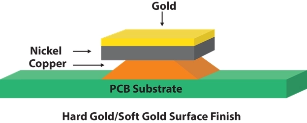
What is Hard Gold / Edge Contacts PCB surface finish? (99.6% purity)
Hard gold is plated over the nickel, which holds up well and doesn’t break down easily compared to other finishes. Because of its durability, this type of PCB plating is used in applications that involve mechanical contact, such as buttons and keypads.
Hard Gold: Min. Gold thickness for Class 1 & 2 boards is 0.8 μm, and for Class 3 boards 1.25 μm. Minimum Nickel thickness for Class 1 boards is 2 μm, and for Class 2 & 3 boards 2.5 μm. Shelf life: 12 months
Advantage of Hard Gold surface finish:
1. Durable surface resistant to mechanical friction. This is where it performs best.
2. Long service life
3. RoHS compliant
Disadvantage of Hard Gold surface finish:
1. Expensive
2. Poor solderability, therefore selective plating only is recommended.
The thickness of the hard gold surface finish will vary depending on the applications. When hard gold is used for compliance in military applications, the minimum thickness shall be 50 -100 micro inch.
Nonmilitary applications require 25 to 50 micro inches. Here are the recommended minimum and maximum thickness values:
- 17.8 μin is recommended for IPC maximum solderable thickness
- 25 μin gold over 100 μin nickel for IPC Class 1 & Class 2 applications
- 50 μin gold over 100 μin nickel for IPC Class 3 applications

What is Soft Gold Surface Finish
Soft Gold is also known as Electrolytic Wire Bondable Gold. A soft gold finish, as the name suggests, contains a higher gold purity on the outer gold plating. Soft gold has a 99.9% purity.
Soft gold finish is used for boards designed mostly for applications that require wire bonding, high solderability and weldability. Soft gold produces a much stronger welded joint when compared to hard gold.
Advantages of Electrolytic Wire Bondable Gold / Soft Gold
1. Has a long shelf life
2. Allows for strong joints
3. Ensures strong connections
Disadvantages of Electrolytic Wire Bondable Gold / Soft Gold
1. Can be expensive
2. Not widely available
Crucial Factors in Selecting Your PCB Finish
NFKDFDGFSdf (160)