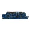
This 8-layer FR4 PCB addresses the challenges of high-density, narrow-format electronic designs, where space efficiency and signal integrity are critical. With dimensions of 165.50×25.90mm and a 1.6MM 두께, the board provides a compact yet robust platform for integrating complex circuitry in applications such as industrial sensors, communication modules, and portable test equipment. 건축 FR4 material, it offers stable electrical insulation (dielectric constant εr=4.5) and mechanical strength, suitable for operation in environments with moderate temperature and vibration.

Layer Architecture & Signal Integrity

  • 8-Layer Stackup:
    • 4 신호 레이어 + 4 power/ground planes for efficient EMI suppression
    • Alternating signal and power planes minimize cross-talk and impedance variations
  • 1온스 (35μm) 구리 두께:
    • Balances fine-line routing (최소 선/공간: 75μm/75μm) with current-carrying capacity (up to 8A per trace)
  • Precision Impedance Control:
    • 50Ω ±8% for microstrip/stripline configurations
    • Critical for maintaining signal integrity in high-speed interfaces (예를 들어, USB 3.0, CAN FD)

High-Density Design Features

  • Blue LPI Solder Mask:
    • Distinctive color for easy visual inspection in narrow layouts
    • Chemical resistance against industrial contaminants
  • ENIG Surface Finish:
    • 3–5μm nickel layer for corrosion resistance
    • 0.05–0.1μm gold layer for long-term solderability and wire bonding compatibility
  • Mixed SMT+DIP Assembly:
    • SMT support for high-density ICs (예를 들어, microcontrollers, FPGAs)
    • DIP compatibility for rugged connectors (예를 들어, 0.1” headers, terminal blocks) and through-hole components

조작 & 품질 관리

  • High-Precision Fabrication:
    • Laser direct imaging (LDI) for 75μm trace accuracy
    • Electrolytic copper plating with ±5% thickness uniformity
  • Comprehensive Testing:
    • 100% AOI inspection for solder mask and silkscreen quality
    • X-ray verification of BGA vias
    • Flying probe testing for electrical continuity and isolation
  • Environmental Compliance:
    • IPC-6012 클래스 2 for industrial applications
    • RoHS/REACH compliant for hazardous substance restrictions
    • Thermal cycling tested (-40°C to +85°C, 500 cycles)

응용 프로그램

  • Industrial Sensor Modules:
    Supports high-density sensor interfaces, signal conditioning, and communication protocols (예를 들어, Modbus, Profibus) in a narrow form factor.
  • Communication Gateways:
    Enables multi-protocol conversion (예를 들어, Ethernet to RS-485) with compact PCB real estate.
  • Portable Test Equipment:
    Integrates measurement circuitry and user interfaces in handheld devices.
  • Automotive Control Units:
    Fits into space-constrained compartments while maintaining signal integrity in harsh environments.


By integrating 8-layer signal isolation, 1OZ copper conductivity, and ENIG durability, this PCB delivers uncompromised performance in demanding, space-constrained applications. The blue solder mask offers visual distinction in complex layouts, while mixed SMT/DIP assembly supports both high-density digital components and robust field connections. ISO에 의해 지원됩니다 9001:2015 certification, it provides the foundation for reliable, compact electronic systems requiring both performance and durability.

PCB 기능


표준 PCB 맞춤형 PCB
레이어 수 2-20 2-50
재료 FR4 대만 연합의 고속 재료, 그리고 기술, Rogers 등의 고주파 재료.
PCB 두께 0.4-3.2mm 0.4-6.4mm
구리 중량 가져 오기 -3o 가져 오기 10
최소. 구멍 직경 0.3mm 0.1레이저 드릴에 의한 MM
PCB 크기 최소. 6.00x6.00mm 최대. 600.00x620.00mm
PCB 마감 할, Hal-Leadfree, 동의하다, Enepic, 침지 주석, 침수은, OSP
Min.Soldermask 댐. 41oz에 대한 MILS 2.51oz에 대한 MILS
Prepreg 유형 2116,1080 2116,1080,7628,3313,106
Min.Width/Space 4/4 밀스 2.5/2.5 밀스
최소. 환형 반지 4/4 밀스 2.5/2.5 밀스
종횡비 8:1 15:1
리드 타임 2 주 5 날 - 5 주
임피던스 공차 ±5% - ±10% ±5% - ±10%
다른 기술 금 손가락, 맹인과 묻힌 구멍, 껍질을 벗길 수있는 솔더 마스크, 가장자리 도금, 카본 마스크, 카운터 싱크 구멍,
반/카스텔 화 구멍, Fit Hole을 누릅니다, 수지로 꽂고 채워진 것을 통해, 패드를 통해 (요일, POFV), 하나의 PCB에서 다재다능합니다

이것은 닫힙니다 0

PCBA 기능


아니요. 프로세스 기능 매개 변수
1 주문 수량 1pc 이상
2 PCB 유형 강성 PCB, FPC, RIDID-FLEX PCB
3 어셈블리 기술 smt, tht, 혼합 기술 또는 팝
4 구성 요소 소싱 완전한 턴키, 부분적인 턴키, 위탁
5 PCB 크기 45*45mm -- 510*500mm
6 BGA 패키지 bga 그녀. 0.14mm, BGA 0.2mm 피치
7 부품 프레젠테이션 줄자, 릴, 스틱 또는 트레이
8 철사 & 케이블 와이어 하네스 및 케이블 어셈블리
9 품질 검사 시각적, SPI, FAI, AOI; 엑스선 점검
10 장착 정확도 ±0.035mm (±0.025mm)
11 최소 패키지 01005 (0.4mm*0.2mm)
12 적합성 코팅 머신에서 사용할 수 있습니다
13 IC 검사 기능, 전기 또는 삭제 테스트
14 리드 타임 3 날 - 5 주
15 다른 기술 박스 빌드 어셈블리, IC 프로그래밍, 구성 요소 비용 다운, 기능 & 노화 테스트 커스텀으로서,
Fit Assembly를 누릅니다, SAC305 또는 더 나은 솔더 페이스트 사용, BGA realling 또는 재 작업,
EMI 방출 제어를위한 방패 덮개 어셈블리

이것은 닫힙니다 0

FPC 기능


아니요. 프로세스 기능 매개 변수
1 레이어 수 1-8 레이어
2 FPC 자료 pi, 애완 동물, 펜, FR-4
3 최종 두께 0.06-4.0mm
4 보드 크기 250.00x1200mm
5 구리 호일 12하나,18하나,35하나,70하나
6 최소 폭/공간 3천/3mil
7 홀로 볼 구리 두께 8-20μm
8 표면 처리 홀 리드 드리, 동의하다, 몰입은/주석, OSP
9 차원을 개요합니다 ± 2mil
10 솔더 내열 저항 280℃ / 10SECS
11 보강재 유형 pi, FR4, 스테인레스 스틸, 알류미늄
12 최소. 홀 데이 (PTH) 0.1mm ± 3mils
13 최소. 홀 데이 (npth) 0.25± 2mil
14 최대/최소 솔더 마스크 두께 2MIL/0.5mil (501/12.7um)
15 최소 슬롯 0.8mm × 1mm

이것은 닫힙니다 0