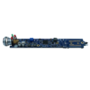
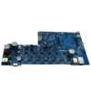
This 4-layer FR4 PCB addresses the needs of industrial control and automation systems that require a balance of compact design, reliable performance, and versatile component integration. With dimensions of 107.03×42.80mm and a 1.6MM 두께, the board offers a space-efficient platform for mounting microcontrollers, communication interfaces, and power management components in devices such as sensor nodes, motor controllers, and industrial gateways. 건축 FR4 material, it provides stable electrical insulation (dielectric constant εr=4.5) and mechanical rigidity, suitable for operation in environments with moderate vibration and temperature fluctuations.

Layer Architecture & Power-Signal Separation

  • 4-Layer Stackup:
    • 2 신호 레이어 + 2 power/ground planes to minimize electromagnetic interference (에미)
    • Inner layers optimized for split power domains (예를 들어, 5V/3.3V) and ground plane isolation
  • 1온스 (35μm) 구리 두께:
    • Supports moderate current loads (넓은 흔적 당 최대 8A) for power-hungry components
    • Copper pour areas on power planes reduce voltage drop and thermal hotspots

Industrial-Grade Design Features

  • Blue LPI Solder Mask:
    • Enhances visual contrast for component identification in dense layouts
    • Chemical resistance against industrial solvents and cleaning agents
  • ENIG Surface Finish:
    • 3–5μm nickel layer prevents corrosion in harsh environments
    • 0.05–0.1μm gold layer ensures reliable solder joints for both SMT and DIP components
  • Mixed SMT+DIP Capability:
    • smt: High-density placement of 0201 passive components, QFP ICs, and BGA packages (0.5mm pitch)
    • DIP: Through-hole mounting for rugged connectors (예를 들어, terminal blocks, RJ45 ports) and relays

조작 & 품질 관리

  • Precision Fabrication:
    • Laser direct imaging (LDI) for 75μm line/space accuracy in signal traces
    • Electrolytic copper plating with uniform thickness across all layers
  • Comprehensive Testing:
    • 100% automated optical inspection (AOI) for solder mask coverage and silkscreen clarity
    • Flying probe testing for electrical continuity (≤0.1o) 그리고 격리 (≥100mΩ)
    • Thermal cycling (-40°C to +85°C, 500 cycles) to verify reliability
  • Standards Compliance:
    • IPC-6012 클래스 2 for industrial electronics
    • ROHS/REACH는 무연 및 위험 물질 제한을 준수합니다

산업 응용 분야

  • Industrial IoT Sensors:
    Integrates temperature/humidity sensors, wireless modules (Wi-Fi/Bluetooth), and data processing circuitry.
  • Motor Control Modules:
    Manages low-voltage motors in conveyor systems, with PWM control and current sensing.
  • Communication Gateways:
    Enables protocol conversion (예를 들어, RS-485 to Ethernet) for smart factory networks.
  • Portable Test Equipment:
    Supports compact measurement devices for on-site industrial diagnostics.


By combining 4-layer signal isolation, 1OZ copper conductivity, and mixed assembly flexibility, this PCB enables engineers to build robust industrial control systems in a compact form factor. The blue solder mask and ENIG finish balance visual identification with long-term reliability, while the 107.03×42.80mm layout optimizes space for both high-density components and field-wired connections. ISO에 의해 지원됩니다 9001:2015 certification, it delivers consistent performance for applications where size, 내구성, and functionality are critical.

PCB 기능


표준 PCB 맞춤형 PCB
레이어 수 2-20 2-50
재료 FR4 대만 연합의 고속 재료, 그리고 기술, Rogers 등의 고주파 재료.
PCB 두께 0.4-3.2mm 0.4-6.4mm
구리 중량 가져 오기 -3o 가져 오기 10
최소. 구멍 직경 0.3mm 0.1레이저 드릴에 의한 MM
PCB 크기 최소. 6.00x6.00mm 최대. 600.00x620.00mm
PCB 마감 할, Hal-Leadfree, 동의하다, Enepic, 침지 주석, 침수은, OSP
Min.Soldermask 댐. 41oz에 대한 MILS 2.51oz에 대한 MILS
Prepreg 유형 2116,1080 2116,1080,7628,3313,106
Min.Width/Space 4/4 밀스 2.5/2.5 밀스
최소. 환형 반지 4/4 밀스 2.5/2.5 밀스
종횡비 8:1 15:1
리드 타임 2 주 5 날 - 5 주
임피던스 공차 ±5% - ±10% ±5% - ±10%
다른 기술 금 손가락, 맹인과 묻힌 구멍, 껍질을 벗길 수있는 솔더 마스크, 가장자리 도금, 카본 마스크, 카운터 싱크 구멍,
반/카스텔 화 구멍, Fit Hole을 누릅니다, 수지로 꽂고 채워진 것을 통해, 패드를 통해 (요일, POFV), 하나의 PCB에서 다재다능합니다

이것은 닫힙니다 0

PCBA 기능


아니요. 프로세스 기능 매개 변수
1 주문 수량 1pc 이상
2 PCB 유형 강성 PCB, FPC, RIDID-FLEX PCB
3 어셈블리 기술 smt, tht, 혼합 기술 또는 팝
4 구성 요소 소싱 완전한 턴키, 부분적인 턴키, 위탁
5 PCB 크기 45*45mm -- 510*500mm
6 BGA 패키지 bga 그녀. 0.14mm, BGA 0.2mm 피치
7 부품 프레젠테이션 줄자, 릴, 스틱 또는 트레이
8 철사 & 케이블 와이어 하네스 및 케이블 어셈블리
9 품질 검사 시각적, SPI, FAI, AOI; 엑스선 점검
10 장착 정확도 ±0.035mm (±0.025mm)
11 최소 패키지 01005 (0.4mm*0.2mm)
12 적합성 코팅 머신에서 사용할 수 있습니다
13 IC 검사 기능, 전기 또는 삭제 테스트
14 리드 타임 3 날 - 5 주
15 다른 기술 박스 빌드 어셈블리, IC 프로그래밍, 구성 요소 비용 다운, 기능 & 노화 테스트 커스텀으로서,
Fit Assembly를 누릅니다, SAC305 또는 더 나은 솔더 페이스트 사용, BGA realling 또는 재 작업,
EMI 방출 제어를위한 방패 덮개 어셈블리

이것은 닫힙니다 0

FPC 기능


아니요. 프로세스 기능 매개 변수
1 레이어 수 1-8 레이어
2 FPC 자료 pi, 애완 동물, 펜, FR-4
3 최종 두께 0.06-4.0mm
4 보드 크기 250.00x1200mm
5 구리 호일 12하나,18하나,35하나,70하나
6 최소 폭/공간 3천/3mil
7 홀로 볼 구리 두께 8-20μm
8 표면 처리 홀 리드 드리, 동의하다, 몰입은/주석, OSP
9 차원을 개요합니다 ± 2mil
10 솔더 내열 저항 280℃ / 10SECS
11 보강재 유형 pi, FR4, 스테인레스 스틸, 알류미늄
12 최소. 홀 데이 (PTH) 0.1mm ± 3mils
13 최소. 홀 데이 (npth) 0.25± 2mil
14 최대/최소 솔더 마스크 두께 2MIL/0.5mil (501/12.7um)
15 최소 슬롯 0.8mm × 1mm

이것은 닫힙니다 0