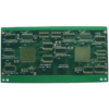
10-계층 임피던스 제어 FR4 PCB는 정확한 신호 무결성이 필요한 고속 전자 시스템을 위해 설계되었습니다., 데이터 센터와 같은, 네트워크 장비, 고급 통신 장치. 다층 구조가 결합됩니다 10 FR4 기판의 층 (1.6MM 총 두께) 고밀도 회로에 대한 복잡한 라우팅을 가능하게합니다, 동안 BGA (볼 그리드 어레이) 막힌 vias와 함께 중요한 구성 요소에 대한 신뢰할 수있는 상호 연결을 보장합니다. 그만큼 50ω ± 8% 임피던스 제어 신호 반사 및 크로스 토크를 최소화합니다, PCIE와 같은 고주파 애플리케이션에 이상적입니다 4.0, USB 3.2, 또는 이더넷 시스템.
그만큼 동의하다 (전기 전기 니켈 몰입 금) 표면 처리는 매끄럽게 제공됩니다, 산화 방지 마감, 납땜 가능성 및 장기 신뢰성 향상. FR4 재료는 비용 효율성과 전기적 안정성의 균형을 제공합니다. (유전 상수 εR = 4.5), 상업용 및 산업 모두에 적합합니다. 우리의 고급 제조 공정에는 포함됩니다:
- 레이저 직접 이미징 (LDI) 미세한 정밀도 (최소 선 너비/공간: 50µm/50mm)
- 자동 임피던스 테스트 각 층에서 ± 8% 공차 준수를 보장합니다
- 100% AOI (자동화 된 광학 검사) 결함 검출을위한 비행 프로브 테스트
ISO로 9001:2015 인증 된 제조업체, 우리는 제공합니다 DFM (제조 가능성을위한 설계) 생산 설계를 최적화하기위한 분석, 비용과 리드 시간을 줄입니다. 이 PCB는 고성능을 원하는 엔지니어에게 이상적입니다, 차세대 전자 제품을위한 신뢰할 수있는 솔루션.

")