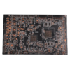
Ce PCB FR4 TG170 à 6 couches offre des performances élevées pour l'automatisation industrielle, 5Modules de communication G, et autres appareils électroniques essentiels à la mission. Doté d'une épaisseur de 1,6 mm, 1Cuivre OZ sur toutes les couches, et une finition de surface ENIG, il équilibre la stabilité thermique, Intégrité du signal, et durabilité mécanique efficace.
Parce qu'il utilise du matériau FR4 avec une Tg de 170°C, ce PCB résiste aux environnements industriels difficiles comme les usines, pôles de communication extérieurs, et systèmes automobiles. Sa conception à 6 couches comprend 4 couches de signaux et 2 Alivins de puissance / sol, qui réduisent activement les interférences électromagnétiques (EMI). Donc, il assure une transmission stable des données dans des applications telles que les automates, passerelles IoT industrielles, et stations de base sans fil.
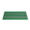
Une caractéristique clé est le doigt en or avec 2 placage micropouce, qui offre une excellente résistance à la corrosion et des contacts électriques durables. Cette conception convient aux systèmes nécessitant une insertion/retrait fréquente de la carte, y compris les systèmes industriels modulaires et les dispositifs de communication montés en rack. En outre, la finition ENIG améliore la soudabilité et la liaison des fils. Il utilise une barrière de nickel pour empêcher l'oxydation et une fine couche d'or optimisée pour les composants à pas fin..
Nous appliquons un processus de fabrication strict pour garantir précision et cohérence:
Traitement de la couche interne: Imagerie directe laser (LDI) définit de fines traces de 75 μm sur du cuivre de 1 OZ.
Forage & Placage: Perçage mécanique de précision et trous métallisés (Pth) assurer des vias électriques robustes.
Modélisation de la couche externe: Le laminage à film sec et l'étamage protègent les circuits pendant la gravure.
Finition de surface: Le revêtement ENIG combiné à un masque de soudure LPI vert améliore la durabilité et la clarté visuelle.
Contrôle de qualité: Nous effectuons 100% tests électriques (Test électronique) et inspection optique automatisée (AOI) pour garantir des planches sans défauts. Nous rejetons strictement tous les panneaux X-out pour maintenir une haute qualité.
Systèmes de contrôle industriels: Fournit une alimentation fiable et une intégrité du signal pour les automates et les entraînements de moteur.
5G & Communication sans fil: Prise en charge de l'intégrité RF en 5G sous-6 GHz et Wi-Fi 6 appareils.
Dispositifs médicaux: Conforme aux normes RoHS/REACH et de biocompatibilité.
Aérospatial & Défense: Résiste aux vibrations et aux cycles de température dans les environnements difficiles.
Stabilité thermique: Il surpasse la norme FR4 et réduit le risque de délaminage.
Contacts à doigt en or fiables: Garantit une faible résistance et des performances durables.
Conception flexible: Prise en charge des assemblages mixtes SMT/DIP avec compatibilité à pas fin.
Conformité mondiale: Découvrez la classe IPC-6012 2 normes de qualité pour une production de masse cohérente.
Ingénieurs développant l’automatisation intelligente des usines, infrastructures de télécommunications, ou l'électronique médicale de haute fiabilité trouvera que ce PCB offre des performances, évolutivité, et certification nécessaires pour les technologies industrielles et de communication de nouvelle génération.