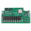
Nous avons conçu ce PCB PCBA double face spécifiquement pour les applications de connectivité d'imprimante, intégrant un circuit imprimé flexible (FPC) capacités technologiques et de programmation IC.
Conçu pour une communication transparente entre les systèmes d'impression, ce PCB FR4 de 1,6 mm convient à tout, des imprimantes domestiques aux machines industrielles. Il offre un support mécanique solide et des performances électriques stables, garantir un fonctionnement fiable dans des environnements exigeants.
Nous avons optimisé l'architecture double face du PCBA pour un routage efficace du signal et une intégration transparente des composants..
- Structure des couches: Le PCB FR4 double face (Tg130°C) prend en charge l'assemblage mixte, avec composants SMT (tels que les MCU et les circuits intégrés de pilote) placé sur la couche supérieure et les composants THT (y compris les connecteurs d'alimentation et les prises FPC) sur la couche inférieure. Le 1OZ (35μm) l'épaisseur du cuivre assure une transmission de courant stable, gérer jusqu'à 3A pour les composants gourmands en énergie.
- Intégration FPC: Équipé de connecteurs FFC/FPC au pas de 0,5 mm (Par exemple, Série JAE LY), le PCBA prend en charge les interfaces 50-100 broches avec un rayon de courbure ≥5 mm, capable de résister à 10,000 cycles de flexion. La flexibilité permet un câblage fiable pour les pièces mobiles de l'imprimante dans un espace limité.
- Programmation IC: Avec programmation intégrée au système (FAI) et interfaces de débogage JTAG/SWD, le PCBA permet le pré-flashing du firmware, y compris les algorithmes de contrôle d'impression et les protocoles de communication. Prend en charge les mises à jour USB et la compatibilité MCU pour les fonctions d'imprimante personnalisées.
Le PCBA est soumis à un processus d'assemblage méticuleux pour garantir précision et fiabilité:
Imprimer Coller et SPI:
Utilisez de la pâte à souder SAC305 sans plomb avec un pochoir découpé au laser de 0,12 mm. 3D SPI garantit la précision du volume de pâte dans 5%, prévention des courts-circuits sur les circuits intégrés à pas fin (0.5pas en mm).
Prendre & Placer et redistribuer:
Pick-and-place de haute précision (±25μm) lieux 0402 composants. La refusion d'azote à 255°C réduit l'oxydation et garantit des joints de soudure fiables.
AOI et THT:
L'inspection optique automatisée détecte le désalignement et les erreurs de polarité avant le soudage à la vague des pièces THT à 250°C. Les joints passent un test de force de traction 3N.
Tests fonctionnels et conformité:
Les tests électriques vérifient l'intégrité du signal (≥10Mbps), ondulation de puissance (≤50mV), et compatibilité des protocoles (USB 2.0, UART).
Les rayons X scannent les circuits intégrés BGA pour garder les vides en dessous 10%.
Les tests environnementaux comprennent 300 cycles thermiques (-20°C à 60°C) et 96 heures de chaleur humide (40°C/93% HR).
- Imprimantes domestiques: Idéal pour les cartes mères d'imprimantes à jet d'encre et laser, le PCBA permet un transfert de données à grande vitesse pour le traitement de l'image et le positionnement précis de la tête d'impression via des connexions FPC.
- Imprimantes d'étiquettes industrielles: Conçu pour résister aux vibrations sur les lignes de production, il prend en charge la génération de codes-barres et de codes QR via une programmation IC personnalisée, garantissant une impression d'étiquettes précise et cohérente.
- Imprimantes thermiques: Utilisé dans les systèmes de point de vente et les dispositifs médicaux, il prend en charge les protocoles de communication USB/série. Les circuits intégrés préprogrammés rationalisent l'intégration, réduire le temps de développement pour les clients.
- Solution à guichet: Offrir des services complets de fabrication de PCB (ligne / espace minimum: 100μm), Approvisionnement des composants (distributeurs agréés pour TI, ST, Murata), Assemblage SMT / THT, Programmation IC, aux tests fonctionnels.
- Personnalisation FPC: Adapte les FPC à des exigences spécifiques, y compris l'épaisseur (0.1-0.3MM), adaptation d'impédance (50Ω/75Ω), couches de blindage (feuille d'aluminium/cuivre), et finitions de surface (placage or/nickel).
- Réponse rapide: Délai standard de 4-5 semaines; Fai (Inspection du premier article) rapports et traçabilité complète du matériel (Conforme RoHS/REACH) sont fournis. Essais en petits lots (100-500 unités) peut être accéléré dans 2 semaines.
PCBA double face personnalisé avec programmation FPC et IC pour une stabilité, connectivité d'imprimante flexible. Que ce soit pour des applications grand public ou industrielles, il établit une norme en matière de connectivité, flexibilité, et fiabilité dans la technologie d'impression.