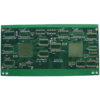
10-Impédance de couche COMMENT COMMENT PCB est conçu pour les systèmes électroniques à grande vitesse nécessitant une intégrité précise du signal, comme les centres de données, équipement réseau, et dispositifs de communication avancés. La structure multicouche combine 10 Couches de substrat FR4 (1.6mm épaisseur totale) pour permettre un routage complexe pour les circuits à haute densité, Pendant que le BGA (Ball Ball Grid Bread) avec des vias branchés assure des interconnexions fiables pour les composants critiques. Le 50Ω ± 8% Contrôle d'impédance minimise la réflexion du signal et la diaphonie, Le faire idéal pour les applications à haute fréquence comme PCIe 4.0, USB 3.2, ou des systèmes Ethernet.
Le Accepter (Or d'immersion nickel électrolaire) Le traitement en surface fournit un lisse, finition résistante à l'oxydation, Amélioration de la soudabilité et de la fiabilité à long terme. Le matériau FR4 offre un équilibre entre rentable et stabilité électrique (constante diélectrique εr = 4,5), Convient à la fois pour un usage commercial et industriel. Notre processus de fabrication avancé comprend:
- Imagerie directe laser (LDI) pour une précision fine (Largeur de ligne minimale / espace: 50µm / 50 mm)
- Test d'impédance automatisée à chaque couche pour assurer une conformité de tolérance à ± 8%
- 100% AOI (Inspection optique automatisée) et tests de sonde volante pour la détection des défauts
En tant qu'ISO 9001:2015 fabricant certifié, Nous offrons DFM (Conception de la fabrication) Analyse pour optimiser votre conception pour la production, Réduire les coûts et les délais. Ce PCB est idéal pour les ingénieurs à la recherche de hautes performances, Solutions fiables pour l'électronique de nouvelle génération.

")