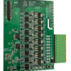
8-La PCB de capa está diseñada para aplicaciones de comunicaciones industriales de misión crítica., donde la integridad de la señal de alta frecuencia, compatibilidad electromagnética (CEM), y una gran durabilidad son esenciales. Con dimensiones de 190mm×170mm y un 1.7MM GRISIÓN, La placa equilibra la integración de componentes a gran escala con la estabilidad mecánica para gabinetes de control industriales y centros de comunicación.. el unico Apilamiento de materiales TU-862+RO4350B combina la resistencia mecánica rentable del TU-862 con las propiedades dieléctricas de baja pérdida del RO4350B (Dk=3,48, tanδ=0,004 a 10 GHz), lo que lo hace ideal para la transmisión de datos de alta velocidad en protocolos como Ethernet, CANabierto, y PROFIBUS.
- Espesor de cobre asimétrico:
- capas exteriores: 1ONZ (35μm) para líneas de energía robustas y blindaje EMI
- capas internas: 0.5ONZ (18μm) para enrutamiento de señales de tono fino
- Permite una distribución equilibrada de la energía. (4 aviones de potencia/terreno) y capas de señal de alta velocidad (4 canales de par diferencial)
- Control de impedancia de precisión:
- 50Ω ± 8% para configuraciones de microstrip/stripline
- Se logra mediante cálculos controlados de espesor dieléctrico y ancho de traza.
- Minimiza la reflexión de la señal en Ethernet de 10 Gbps y en interfaces inalámbricas industriales.
- Vías llenas no conductoras (NCFV) con tapa de cobre:
- Vías rellenas de resina para evitar huecos., luego cubierto con cobre para un acabado superficial liso
- Elimina los riesgos de mecha de soldadura en áreas BGA y mejora la conductividad térmica.
- Laminación secuencial:
- 8 Capas laminadas en etapas para garantizar un espesor dieléctrico uniforme y precisión de registro. (<50μm)
- Acabado superficial de enig:
- 3-5Capa de níquel de μm para resistencia a la corrosión.
- 0.05-0.1Capa de oro de μm para soldabilidad a largo plazo
- Máscara de soldadura LPI verde mate:
- Reduce el deslumbramiento durante la inspección AOI
- Proporciona una resistencia química superior en entornos industriales.
- Mitigación de EMC/EMI:
- Vías de unión del plano de tierra colocadas a intervalos de 2 mm para suprimir el ruido de modo común
- Enrutamiento de pares diferencial de precisión con coincidencia de longitud controlada dentro 5 mils (0.127mm) para garantizar una desviación mínima de la señal
- Gestión Térmica:
- Vías térmicas que conectan los planos de potencia a las capas exteriores para una disipación eficiente del calor.
- Áreas de vertido de cobre en capas de energía para reducir los puntos críticos
- Soporte de montaje mixto:
- SMT para circuitos integrados de alta densidad (P.EJ., chips físicos, FPGAs)
- DIP para conectores resistentes (P.EJ., RJ45, DB25) y relevos
- 100% Pruebas automatizadas:
- Verificación de impedancia por capa
- Inspección por rayos X de vías NCFV
- AOI para máscara de soldadura y calidad de serigrafía
- Pruebas ambientales:
- Ciclos de temperatura (-40° C a +85 ° C, 1,000 ciclos)
- Prueba de vibración (5-500Hz, 2G Aceleración)
- Cumplimiento de estándares:
- Clase IPC-6012 3 para aplicaciones de misión crítica
- RoHS/REACH para restricciones de sustancias peligrosas
- EN 55032 Clase A para emisiones electromagnéticas
- Conmutadores Ethernet industriales:
Admite 10GBASE-T y PoE+ con una mínima degradación de la señal
- Estaciones base inalámbricas:
Permite enrutamiento de radiofrecuencia 5G NR sub-6GHz
- SOCIEDAD ANÓNIMA & Sistemas SCADA:
Facilita el intercambio de datos en tiempo real en las plantas de fabricación.
- Redes de comunicación ferroviaria:
Se encuentra en 50155 Normas medioambientales para aplicaciones de material rodante.

")