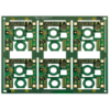
8-La PCB FR4 de capa está diseñada para diseños electrónicos de alta densidad que requieren un equilibrio de integridad de la señal., distribución de energía, y factores de forma compactos, como la electrónica de consumo, dispositivos médicos, y módulos de control industrial. El 8-arquitectura de capa (típicamente 4 capas de señal + 4 aviones de potencia/terreno) permite enrutamiento complejo para componentes de paso fino mientras minimiza la interferencia electromagnética (EMI). El 1.2MM GRISIOR ofrece una base ligera pero rígida, ideal para aplicaciones con espacio limitado donde el peso y la durabilidad son críticos.
Construido con Material FR4, la PCB proporciona un aislamiento eléctrico confiable (constante dieléctrica εr = 4.5) y estabilidad mecánica, adecuado para una amplia gama de entornos operativos. El 2ONZ (70μm) espesor de cobre en todas las capas mejora la capacidad de transporte de corriente (hasta 15a por rastro) manteniendo al mismo tiempo la flexibilidad del diseño para trazas de energía y señal. El IPV verde (Fotoimagen líquida) máscara de soldadura no solo protege los circuitos contra daños ambientales sino que también mejora la precisión de la inspección visual, mientras el Serigrafía blanca Garantiza marcados y designaciones claras de los componentes para el montaje y el mantenimiento..
Una característica clave es la Aceptar (Oro de inmersión de níquel electroutolante) tratamiento superficial, que proporciona una suave, Acabado resistente a la corrosión para una excelente soldabilidad.. La capa de níquel (3–5 μm) agrega durabilidad, y la capa de oro (0.05-0,1 µm) previene la oxidación, haciéndolo adecuado para uso a largo plazo. El POFV (Vías plateadas sobre rellenas) La tecnología mejora aún más la confiabilidad de la PCB: Las vías se llenan con material conductor y se recubren., Eliminación de huecos que podrían causar estrés térmico o absorción de soldadura.. Esto es particularmente importante para diseños de alta densidad con componentes de paso fino. (P.EJ., 0.5BGA de paso de mm) y garantiza un rendimiento constante en los procesos de soldadura por reflujo.
La fabricación de esta PCB implica técnicas avanzadas para garantizar precisión y calidad.:
- Imágenes directas láser (LDI) logra una precisión de línea fina (ancho de línea mínimo/espacio: 50µm/50 µm) para enrutamiento complejo.
- Procesamiento POFV utiliza epoxi o resina conductora para llenar las vías, seguido de enchapado para crear una superficie lisa.
- 100% AOI (Inspección óptica automatizada) verifica la cobertura de la máscara de soldadura y la claridad de la serigrafía.
- Pruebas electricas Garantiza continuidad y resistencia de aislamiento., Cumpliendo con la Clase IPC-6012 2 estándares.
Los ingenieros apreciarán la versatilidad de la PCB para manejar tanto el enrutamiento de señales de alta densidad como aplicaciones de potencia moderada.. En electrónica de consumo, admite diseños compactos para teléfonos inteligentes, tabletas, y wearables, donde el espacio es un bien escaso. En dispositivos médicos, La tecnología POFV y el acabado ENIG contribuyen a la confiabilidad a largo plazo en los equipos de diagnóstico.. En sistemas industriales, El cobre 2OZ y el material FR4 proporcionan la durabilidad necesaria para paneles de control y módulos de automatización..
Al elegir este PCB FR4 de 8 capas con cobre de 2OZ, Acabado ENIG, y tecnología POFV, los clientes obtienen una solución que equilibra la densidad, fiabilidad, y rentabilidad. Su combinación de llenado vía avanzada, tratamiento superficial premium, y la fabricación precisa lo convierte en una opción estratégica para aplicaciones donde la integración de componentes y el rendimiento a largo plazo son esenciales. Respaldado por ISO 9001:2015 proceso de dar un título, Esta PCB garantiza una calidad constante desde la creación de prototipos hasta la producción en masa..

")