

En el complejo mundo de la electrónica, placas de circuito impreso (PCBS) Servir como el sistema nervioso de todo el hardware.. Whether it’s precision consumer electronics or rugged industrial control systems, their core relies on the thousands of components mounted on a PCB. Sin embargo, ensuring that these components are accurately procured, assembled, tested, and maintained requires a clear understanding of their identification.
This is especially true for surface-mount devices (SMD) and through-hole technology (Tht) componentes, which have distinct marking methods on the PCB. These differences directly impact a product’s functionality, fiabilidad, and production efficiency.
Failure to correctly identify components can lead to decreased manufacturing efficiency at best, and product malfunctions or even safety hazards at worst. This article will delve into the identification characteristics of SMD and through-hole components on PCBs, the role of the silkscreen layer, and how [Totalmente Hong] ensures every component is accurately marked through professional design and manufacturing processes, supporting the success of your projects.

1. Identification Features of Surface-Mount Devices (SMD) ✅
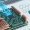
SMD components are the cornerstone of miniaturization and integration in modern electronic products. They are typically small in size, lack traditional leads, and are directly mounted onto PCB pads. Due to their compact dimensions, the markings on SMD components are often very minimal, and some very small components may have no visible identification at all.
Component Markings: Most SMD components, especially integrated circuits (IM), transistors, and larger resistors or capacitors, have markings on their black or gray bodies, including the manufacturer’s logo, número de parte, and batch information. These codes usually require reference to the manufacturer’s datasheet for full interpretation. Por ejemplo, a simple three- or four-digit code might indicate a resistor’s value or a capacitor’s capacitance. For ICs, a dot or chamfer typically marks the direction of Pin 1.
Size and Package: The package type of an SMD component (como 0402, 0603, COMPENSACIÓN, QFN, etc.) is itself an important identification feature, determining both the physical size and pin layout of the component.
Unmarked Components: It is worth noting that some extremely small SMD components, such as resistors or capacitors in 0201 o 01005 paquetes, are too tiny to carry any markings on the body. In these cases, the silkscreen reference designators on the PCB and the BOM (Materiales) become the only reliable means of identification.

2. Identification Features of Through-Hole Components (Tht) ⚡
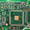
Through-hole components have a longer history and are mounted by inserting their leads through holes in the PCB, then soldering on the opposite side. Compared to SMD components, through-hole components are generally larger, which allows for more comprehensive markings and easier identification.
Component Markings: Through-hole components, such as large electrolytic capacitors, power resistors, conectores, relevos, and DIP-packaged ICs, typically have clear markings on their bodies, including full part numbers, rated parameters (P.EJ., Voltaje, capacidad, resistencia), manufacturer information, and production date. Polarized components, such as electrolytic capacitors and diodes, feature clear polarity indicators—for example, a stripe or arrow marking the negative side of an electrolytic capacitor.
Leads and Shape: The number and arrangement of leads, along with the overall physical shape of the component (P.EJ., round, square, rectangular), also provide important identification cues.
PCB Silkscreen Coordination: Through-hole components are usually closely aligned with the PCB silkscreen reference designators (such as R1, C2, U3) to achieve dual identification. The outline on the silkscreen layer often matches the component’s body shape, facilitating accurate placement.

3. The Critical Role of PCB Silkscreen in Component Identification 📢
For both SMD and through-hole components, the PCB silkscreen layer is vital for identification, asamblea, pruebas, y reparar. It uses printed characters and outlines to guide placement.
-
Designadores de referencia: Codes like “R1,” “C10,” or “U5” link each part to the BOM and its position.
-
Polaridad & Orientation: Marks show diode polarity, capacitor terminals, and IC Pin 1 direction to avoid errors.
-
Component Outlines: Silkscreen shapes help operators or machines place parts accurately.
-
Optimización del diseño: [Totalmente Hong] ensures clear, readable silkscreen during DFM/DFA, avoiding overlaps with pads or vias to reduce assembly mistakes.
4. Key Technical Details and Identification Challenges 🔎
Even with clear markings, practical production and maintenance often encounter identification challenges. Understanding these challenges and knowing how to address them is crucial for improving efficiency and quality.
Polarity and Orientation Errors: One of the most common assembly mistakes occurs with SMD components. Even with silkscreen markings, careless handling can result in reverse installation. For integrated circuits, incorrect Pin 1 orientation can potentially damage or destroy the chip.
Difficulty Identifying Small Components: As mentioned earlier, ultra-small SMD components may have no markings on the body, relying entirely on the silkscreen and BOM for identification. During maintenance, if the silkscreen is damaged, identifying these components becomes significantly more difficult.
Batch and Date Codes: These markings are essential for tracing product quality and assessing component aging. Correct interpretation requires professional knowledge and supporting data.
Coordination Between Gerber Files and BOM: During manufacturing and assembly, operators typically reference both the BOM (Materiales) and Gerber files (PCB design data containing all layer information) to verify component information. The BOM provides detailed information on part numbers, paquetes, and quantities, while the Gerber file provides physical location and silkscreen layer data. Combining the two ensures error-free component identification.
Technical Term Explanation – Gerber File: The standard data format for PCB manufacturing, containing information for all layers including circuit traces, máscara de soldadura, and silkscreen. It serves as the blueprint for PCB production.
Technical Term Explanation – BOM (Materiales): A detailed list of all raw materials, componentes, and quantities required for a product. The BOM is a critical document for procurement and assembly.
Eligiendo [Totalmente Hong], you will gain:
Professional Technical Expertise: Our experienced engineering team provides technical support ranging from diseño de PCB optimization to complex assembly, ensuring your project has a solid technical foundation from concept to mass production.
Exceptional Quality Assurance: With advanced inspection equipment such as AOI and X-Ray, and strict quality control processes, we ensure every delivered PCBA meets the highest industry standards, with industry-leading accuracy in component identification and assembly.
Efficient and Reliable Supply Chain: Our robust global component sourcing network and meticulous material management effectively shorten lead times and reduce your project risks.
Solución integral: We offer full-chain services including PCB manufacturing, component procurement, Montaje SMT/THT, y pruebas, streamlining your procurement process so you can focus on core business innovation.
Want to learn more about the technical details of PCB assembly? Access our comprehensive technical guides and best practices! Or, if you have any PCB/PCBA project needs, feel free to contact our expert team for customized solutions and professional quotations.


Deja una respuesta