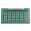
Diese doppelseitige FR4 TG170-Leiterplatte ist eine vielseitige und kostengünstige Lösung. Es eignet sich für Anwendungen von industriellen Steuerungssystemen bis hin zu Unterhaltungselektronik und medizinischen Geräten. Mit einer Dicke von 1,6 mm, 1OZ Kupferschichten, und eine bleifreie HAL-Oberflächenveredelung, Diese Leiterplatte gleicht die mechanische Festigkeit aus, elektrische Zuverlässigkeit, und Umweltkonformität. daher, Es ist ideal für Elektronik mittlerer Komplexität, die eine gleichbleibende Leistung im großen Maßstab erfordert.
Hergestellt aus FR4-Material mit einer hohen Glasübergangstemperatur (Tg) von 170 ° C., Diese Leiterplatte bietet eine verbesserte thermische Stabilität. Im Vergleich zum Standard-FR4 (TG130 ° C.), In Umgebungen mit Temperaturschwankungen zwischen -20 °C und +80 °C ist die Leistung besser. Dieser Vorteil gewährleistet einen zuverlässigen Betrieb. Das doppelseitige Design ermöglicht es Ingenieuren auch, komplexe Schaltkreise effizient zu verlegen. Doppelschichtige Signalleiterbahnen und Kupferfüllungen für Strom- und Masseebenen reduzieren elektromagnetische Störungen (EMI) und die Signalintegrität verbessern. Infolge, Es unterstützt Anwendungen mit niedriger bis mittlerer Geschwindigkeit wie Mikrocontroller, Sensorschnittstellen, und Kommunikationsmodule.
Bleifreie HAL-Oberflächenveredelung: Diese Oberfläche ist RoHS- und REACH-konform. Es bietet eine hervorragende Lötbarkeit und gute Korrosionsbeständigkeit. Zusätzlich, Es eignet sich sowohl für die manuelle als auch für die automatisierte Montage, insbesondere bei Anwendungen, die häufige Nacharbeiten erfordern.
1OZ-Kupferschichten: Mit 35μm Dicke, Die Kupferschichten unterstützen moderate Stromlasten bis zu 8 A pro breiter Leiterbahn. Sie ermöglichen eine feine Linienführung mit einem minimalen Linien-/Abstandsabstand von 100 μm/100 μm. Dies sorgt für ein ausgewogenes Verhältnis zwischen Leistungsabgabe und hoher Komponentendichte.
Grüne LPI-Lötmaske: Die Lötmaske verbessert die visuelle Klarheit bei Montage und Nacharbeit. Darüber hinaus, Es widersteht üblichen industriellen Verunreinigungen wie Ölen, Lösungsmittel, und Reinigungsmittel. daher, Es ist ideal für raue Umgebungen wie Produktionsanlagen oder Outdoor-Geräte.
Die Leiterplatte wird einer präzisen Fertigung unterzogen, um Qualität und Zuverlässigkeit zu gewährleisten:
Hochpräzises mechanisches Bohren mit einer Toleranz von ±50 μm gewährleistet genaue Durchkontaktierungen.
Durchkontaktierte Löcher (PTH) Erhalten Sie eine 25–35 μm dicke Kupferbeschichtung für starke Verbindungen zwischen den Schichten.
Die UV-Lithographie definiert feine Schaltkreismuster mit einer Auflösung von 100 μm.
Die Verzinnung schützt die Leiterbahnen beim Ätzen.
Die langlebige grüne LPI-Lötmaske wird bei 150 °C ausgehärtet.
100% elektrische Tests (E-Test) überprüft Kontinuität und Isolation.
Automatisierte optische Inspektion (Aoi) prüft die Abdeckung der Lötstoppmaske und erkennt Defekte.
Defekte Panels werden grundsätzlich zurückgewiesen, Wir stellen sicher, dass nur einwandfreie Leiterplatten an die Kunden geliefert werden.
Industrielle Steuerung: Geeignet für SPS-Module, Relais-Steuerplatinen, und Sensorschnittstellen, wobei Zuverlässigkeit und Kosteneffizienz im Vordergrund stehen.
Unterhaltungselektronik: Unterstützt intelligente Geräte mit geringem Stromverbrauch, Wearables, und Audiomodule mit kompaktem Design und zugänglichen Testpunkten.
Medizinprodukte: Konform mit RoHS, Es eignet sich für Diagnose- und Überwachungsgeräte, die eine stabile Leistung erfordern.
Prototyping & Ausbildung: Aufgrund der Kompatibilität mit Standard-SMT/DIP-Komponenten beliebt für schnelles Prototyping.
Erfüllt die IPC-6012-Klasse 2 Standards für industrielle Anwendungen.
Vollständig RoHS/REACH-konform.
Auf thermische Belastung getestet (260°C Reflow) und Vibrationsfestigkeit (5-500Hz).
Durch die Kombination eines Substrats mit hoher Tg, bleifreies HAL-Finish, und doppelseitiges Design, Diese Platine liefert eine zuverlässige, skalierbar, und kostengünstige Plattform. Ingenieure entwickeln Industrie, Verbraucher, oder Medizinelektronik finden diese Lösung zuverlässig und konform mit globalen Standards.