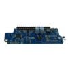
This 8-layer FR4 PCB addresses the challenges of high-density, narrow-format electronic designs, where space efficiency and signal integrity are critical. Mit Dimensionen von 165.50×25.90mm und a 1.6mm Dicke, the board provides a compact yet robust platform for integrating complex circuitry in applications such as industrial sensors, communication modules, and portable test equipment. Gebaut von FR4 -Material, Es bietet eine stabile elektrische Isolierung (Dielektrizitätskonstante εr = 4,5) und mechanische Stärke, Geeignet für den Betrieb in Umgebungen mit mäßiger Temperatur und Vibration.
- 8-Ebenenstapel:
- 4 Signalschichten + 4 Stromversorgungs-/Masseebenen für eine effiziente EMI-Unterdrückung
- Alternating signal and power planes minimize cross-talk and impedance variations
- 1Oz (35μm) Kupferdicke:
- Balances fine-line routing (Mindestlinie/Raum: 75μm/75μm) with current-carrying capacity (bis zu 8a pro Spur)
- Präzise Impedanzkontrolle:
- 50Ω ±8 % für Mikrostreifen-/Streifenleitungskonfigurationen
- Critical for maintaining signal integrity in high-speed interfaces (Z.B., USB 3.0, Kann fd)
- Blaue LPI-Lötmaske:
- Distinctive color for easy visual inspection in narrow layouts
- Chemical resistance against industrial contaminants
- Rätseloberfläche:
- 3–5μm Nickelschicht für Korrosionsbeständigkeit
- 0.05–0,1 μm Goldschicht für langfristige Lötbarkeit und Drahtbondkompatibilität
- Mixed SMT+DIP Assembly:
- SMT support for high-density ICs (Z.B., microcontrollers, FPGAs)
- DIP compatibility for rugged connectors (Z.B., 0.1”Kopfzeilen, Klemmenblöcke) and through-hole components
- Erfindung der hohen Präzision:
- Laser Direct Imaging (LDI) for 75μm trace accuracy
- Electrolytic copper plating with ±5% thickness uniformity
- Umfassende Tests:
- 100% AOI inspection for solder mask and silkscreen quality
- X-ray verification of BGA vias
- Flugsondenprüfung auf elektrische Kontinuität und Isolation
- Umweltkonformität:
- IPC-6012 Klasse 2 for industrial applications
- RoHS/REACH-konform hinsichtlich Gefahrstoffbeschränkungen
- Thermal cycling tested (-40° C bis +85 ° C., 500 Zyklen)
- Industrielle Sensormodule:
Supports high-density sensor interfaces, signal conditioning, and communication protocols (Z.B., Modbus, Profibus) in a narrow form factor.
- Kommunikations-Gateways:
Enables multi-protocol conversion (Z.B., Ethernet to RS-485) with compact PCB real estate.
- Tragbare Testgeräte:
Integrates measurement circuitry and user interfaces in handheld devices.
- Automotive Control Units:
Fits into space-constrained compartments while maintaining signal integrity in harsh environments.
By integrating 8-layer signal isolation, 1OZ Kupferleitfähigkeit, und Rätselbeheblichkeit, this PCB delivers uncompromised performance in demanding, space-constrained applications. The blue solder mask offers visual distinction in complex layouts, while mixed SMT/DIP assembly supports both high-density digital components and robust field connections. Unterstützt von ISO 9001:2015 Zertifizierung, it provides the foundation for reliable, compact electronic systems requiring both performance and durability.