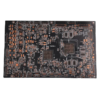
Diese 6-lagige FR4 TG170-Leiterplatte bietet hohe Leistung für die industrielle Automatisierung, 5G-Kommunikationsmodule, und andere geschäftskritische Elektronik. Mit einer Dicke von 1,6 mm, 1Unzen Kupfer auf allen Schichten, und eine ENIG-Oberflächenveredelung, es gleicht die thermische Stabilität aus, Signalintegrität, und mechanische Haltbarkeit effektiv.
Weil FR4-Material mit einer Tg von 170 °C verwendet wird, Diese Leiterplatte hält rauen Industrieumgebungen wie Fabrikhallen stand, Outdoor-Kommunikationsknotenpunkte, und Automobilsysteme. Sein 6-lagiges Design umfasst 4 Signalschichten und 2 Kraft-/Bodenebenen, die elektromagnetische Störungen aktiv reduzieren (EMI). daher, Es sorgt für eine stabile Datenübertragung in Anwendungen wie SPS, Industrielle IoT-Gateways, und drahtlose Basisstationen.
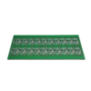
Ein wesentliches Merkmal ist der goldene Finger mit 2 Mikrozoll-Beschichtung, was eine hervorragende Korrosionsbeständigkeit und langlebige elektrische Kontakte bietet. Dieses Design eignet sich für Systeme, die ein häufiges Einsetzen/Entfernen der Platine erfordern, einschließlich modularer Industriesysteme und Rack-montierter Kommunikationsgeräte. Außerdem, Die ENIG-Oberfläche verbessert die Lötbarkeit und das Drahtbonden. Es verwendet eine Nickelbarriere, um Oxidation zu verhindern, und eine dünne Goldschicht, die für Fine-Pitch-Komponenten optimiert ist.
Wir wenden einen strengen Herstellungsprozess an, um Präzision und Konsistenz zu gewährleisten:
Innenschichtverarbeitung: Laser Direct Imaging (LDI) Definiert feine 75μm-Leiterbahnen auf 1OZ Kupfer.
Bohren & Überzug: Präzisionsmechanische Bohrungen und durchkontaktierte Löcher (PTH) sorgen für robuste elektrische Durchkontaktierungen.
Strukturierung der äußeren Schicht: Trockenfilmlaminierung und Verzinnung schützen die Schaltkreise beim Ätzen.
Oberflächenbeschaffung: Die ENIG-Beschichtung in Kombination mit einer grünen LPI-Lötmaske verbessert die Haltbarkeit und visuelle Klarheit.
Qualitätskontrolle: Wir treten auf 100% elektrische Tests (E-Test) und automatisierte optische Inspektion (Aoi) um fehlerfreie Boards zu garantieren. Wir lehnen alle X-out-Panels strikt ab, um eine hohe Qualität zu gewährleisten.
Industrielle Steuerungssysteme: Sorgen Sie für zuverlässige Stromversorgung und Signalintegrität für SPS und Motorantriebe.
5G & Drahtlose Kommunikation: Unterstützt HF-Integrität in 5G Sub-6GHz und Wi-Fi 6 Geräte.
Medizinprodukte: Erfüllen Sie die RoHS/REACH- und Biokompatibilitätsstandards.
Luft- und Raumfahrt & Verteidigung: Beständig gegen Vibrationen und Temperaturwechsel in rauen Umgebungen.
Wärmestabilität: Es übertrifft Standard FR4 und reduziert das Delaminierungsrisiko.
Zuverlässige Goldkontakte: Sorgen Sie für geringen Widerstand und lang anhaltende Leistung.
Flexible Design: Unterstützt gemischte SMT/DIP-Montage mit Fine-Pitch-Kompatibilität.
Globale Compliance: Lernen Sie die IPC-6012-Klasse kennen 2 Qualitätsstandards für eine konsequente Massenproduktion.
Ingenieure entwickeln intelligente Fabrikautomation, Telekommunikationsinfrastruktur, oder hochzuverlässige medizinische Elektronik werden feststellen, dass diese Leiterplatte Leistung bietet, Skalierbarkeit, und Zertifizierung, die für Industrie- und Kommunikationstechnologien der nächsten Generation erforderlich ist.