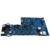
This 2-layer FR4 PCB balances space efficiency with robust performance for industrial control modules, sensor nodes, and low-power automation systems. With dimensions of 98.45×79.69mm and a 1.6mm Dicke, the board offers a versatile platform for integrating microcontrollers, communication interfaces, and power components in a compact form factor. Constructed from FR4 material, it ensures stable electrical insulation (Dielektrizitätskonstante εr = 4,5) and mechanical rigidity, suitable for operation in moderate-temperature industrial environments.

Layer Architecture & Electrical Design

  • 2-Layer Stackup:
    • Top and bottom signal layers with ground/power planes implemented via copper pours for basic EMI suppression.
    • Split power domains (e.g., 5V/3.3V) separated by isolation traces to minimize cross .
  • 1Oz (35μm) Copper Thickness:
    • Supports up to 8A current in power traces (≥1mm width) and fine-line routing (min line/space: 100μm/100μm) for signal integrity.
    • Copper pour areas on both layers reduce thermal hotspots in power-critical sections.

Industrial-Grade Features

  • Green LPI Solder Mask:
    • Standard industrial color for easy visual inspection and component identification.
    • Chemical resistance against common industrial contaminants and cleaning agents.
  • ENIG Surface Finish:
    • 3–5μm nickel layer prevents corrosion; 0.05–0.1μm gold layer ensures reliable solder joints for both SMT and DIP components.
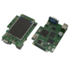
  • SMT+DIP Mixed Assembly:
    • SMT: Accommodates 0402 passive components, SOIC/SSOP ICs, and 0.5mm pitch QFP packages.
    • DIP: Supports through-hole connectors (e.g., 0.1″ headers, terminal blocks) and relays for field wiring.

Manufacturing & Qualitätskontrolle

  • Precision Fabrication:
    • Laser direct imaging (LDI) for 100μm trace accuracy; electrolytic copper plating with uniform thickness verification.
    • V-cut scoring for optional panelization in high-volume orders.
  • Rigorous Testing:
    • 100% automated optical inspection (Aoi) for solder mask coverage and silkscreen clarity.
    • Flying probe testing for electrical continuity (≤0.1Ω) and isolation (≥100MΩ).
    • Wärmespannungstest (260°C reflow cycles) to ensure solder joint reliability.
  • Standards Compliance:
    • IPC-6012 Class 2 for industrial electronics; RoHS/REACH compliant for lead-free manufacturing.

Industrial Applications

  • Industrial Sensor Nodes:
    Integrates temperature/humidity sensors, analog-to-digital converters, and wireless modules (Zigbee/Bluetooth).
  • Motor Driver Modules:
    Manages low-voltage DC motors with PWM control, current sensing, and overheat protection.
  • Communication Interfaces:
    Enables RS-232/485 to USB conversion or simple protocol bridges for legacy industrial equipment.
  • Power Distribution Blocks:
    Distributes 24V DC to multiple loads with circuit protection and status indication.

PCB -Fähigkeit


Artikel Standard -PCB Customized PCB
Anzahl der Schichten 2-20 2-50
Material FR4 Hallo Geschwindigkeitsmaterial von Taiwan Union, Und Technik, Hochfrequenzmaterial von Rogers usw..
Dicke der Leiterplatte 0.4-3.2mm 0.4-6.4mm
Kupfergewicht Bring-3o Bring-10
Min. Lochdurchmesser 0.3mm 0.1MM durch Laserbohrer
PCB -Größe Min. 6.00X6.00 mm max. 600.00X620.00 mm
PCB -Finish Hal, Hal-Leadfree, Zustimmen, Enepic, Eintauchen, Eintauchen Silber, OSP
Min.Soldmask Dam. 4mils für 1oz 2.5mils für 1oz
Prepreg -Typ 2116,1080 2116,1080,7628,3313,106
Min.Width/Space 4/4 Mils 2.5/2.5 Mils
Min. Ringring 4/4 Mils 2.5/2.5 Mils
Seitenverhältnis 8:1 15:1
Vorlaufzeit 2 Wochen 5 Tage - 5 Wochen
Impedanztoleranz ±5% - ±10% ±5% - ±10%
Andere Techniken Goldene Finger, Blinde und vergrabene Löcher, Schälbare Lötmaske, Kantenbeschichtung, Kohlenstoffmaske, Countersink Loch,
Halb-/Castellated -Loch, Drücken Sie das Fit -Loch, Über verstopfte/gefüllt mit Harz, Via in pad (VIP, POFV), Multifinishes auf einer PCB

Dies schließt sich in 0Sekunden

PCBA -Fähigkeit


NEIN. Artikel Prozessfunktionsparameter
1 Bestellmenge Mehr als 1pcs
2 PCB -Typ Starre PCB, FPC, Starr-Flex-PCB
3 Assembly Tech SMT, Tht, Gemischte Technologie oder Pop
4 Komponentenbeschaffung Vollständiger schlüsselfertig, Teilweise schlüsselfertig, Vergeben
5 PCB -Größe 45*45mm -- 510*500mm
6 BGA -Paket BGA sie. 0.14mm, BGA 0,2 mm Tonhöhe
7 Teilepräsentation Band, Spule, Stock oder Tablett
8 Draht & Kabel Kabelbaum und Kabelbaugruppe
9 Qualitätsinspektion Visuell, Spi, Fai, Aoi; Röntgenprüfung
10 Montagegenauigkeit ±0.035mm (±0.025mm)
11 Min -Paket 01005 (0.4mm*0,2 mm)
12 Konforme Beschichtung Erhältlich von Maschine
13 IC -Inspektion Funktion, Elektrik- oder Dekap -Test
14 Vorlaufzeit 3 Tage - 5 Wochen
15 Andere Techniken Box -Build -Baugruppe, IC -Programmierung, Komponenten kosten dankbar, Funktion & Alterungstest als Brauch,
Drücken Sie die Anpassungsbaugruppe, SAC305 oder bessere Lötpaste verwendet, BGA -Neuballer oder Nacharbeit,
Schildabdeckungsbaugruppe für die EMI -Emissionskontrolle

Dies schließt sich in 0Sekunden

FPC -Fähigkeit


NEIN. Artikel Prozessfunktionsparameter
1 Schichtzahl 1-8 Schichten
2 FPC -Material PI, HAUSTIER, STIFT, FR-4
3 Enddicke 0.06-4.0mm
4 Brettgröße 250.00X1200 mm
5 Kupferfolie 12eins,18eins,35eins,70eins
6 Min Breite/Raum 3Tausend/3mil
7 Lochwall Kupferdicke 8-20μm
8 Oberflächenbehandlung Hall Leaddree, Zustimmen, Eintauchen Silber/Zinn, OSP
9 Umrissen Dimension ± 2mil
10 Lötwärmewiderstand 280℃ / 10Secs
11 Versteifungstyp PI, FR4, Edelstahl, Aluminium
12 Min. Lochtag (PTH) 0.1mm ± 3mil
13 Min. Lochtag (Npth) 0.25± 2mil
14 Max/min Soldatendicke 2Mil/0,5 Mio. (50eins/12.7um)
15 Min Slot 0.8mm × 1mm

Dies schließt sich in 0Sekunden