
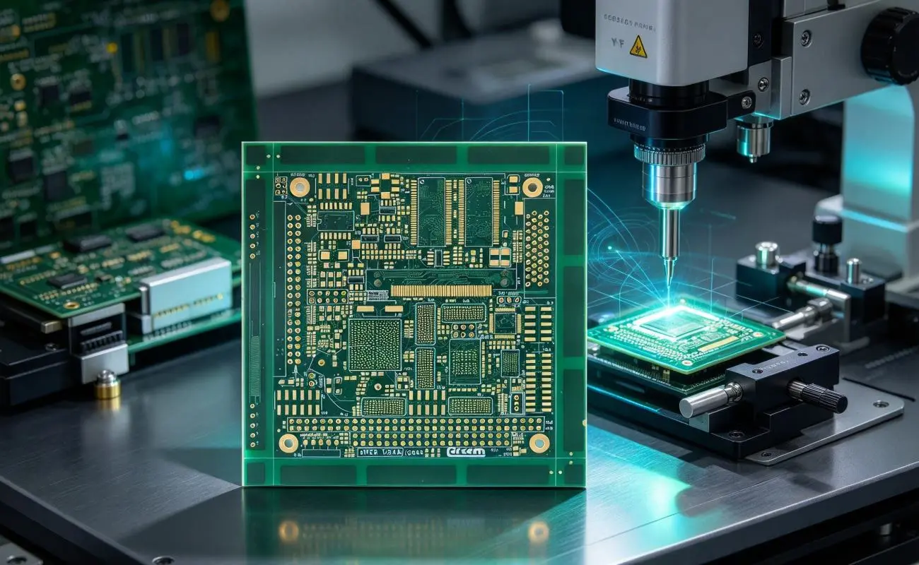
Data centers rely on high-speed electronic systems to process, transmit, and store large volumes of information. As network traffic increases, circuit boards must handle faster data transmission while controlling signal reflection, Übersprechen, und elektromagnetische Störung. A 10-layer impedance-controlled PCB helps address these challenges through multiple routing layers and precise electrical design. Folglich, it supports complex circuits in servers, Netzwerkausrüstung, and advanced communication systems.
How a 10-Layer Structure Supports High-Speed Routing
A multilayer PCB uses conductive layers to route signals, distribute power, and establish ground references. With ten layers, engineers can arrange high-speed signal paths more flexibly. They can also separate sensitive circuits from other routing areas. daher, a 10-layer FR4 PCB design can support high-density applications that require both routing space and stable electrical performance. Jedoch, adding more layers alone does not guarantee signal integrity. Engineers must carefully plan the stack-up, Kupferdicke, dielectric properties, trace geometry, and spacing between adjacent signals. By coordinating these factors during PCB design, manufacturers can produce boards that meet the electrical requirements of high-speed systems.
The Role of 50-Ohm Impedance Control
Controlled impedance helps maintain consistent signal transmission along a PCB trace. When trace impedance differs significantly from connected components or transmission paths, part of the signal may reflect toward its source. This reflection can affect signal quality. A 50-ohm impedance control specification suits certain high-frequency signal paths, although the required value depends on the interface and system design. For this reason, engineers should follow the applicable interface specifications instead of applying one impedance value to every signal.
This product specifies an impedance tolerance of 50Ω ±8%. Manufacturers can adjust trace width, Kupferdicke, dielectric spacing, and material characteristics to achieve the target impedance. Zusätzlich, impedance testing helps verify whether the finished traces meet the agreed requirements.
BGA Plugged Vias for Reliable Interconnections
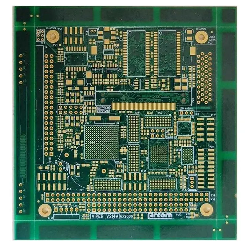
High-density components, such as Ball Grid Array (BGA) Pakete, require carefully designed connections between component pads and internal PCB layers. A BGA plug-in vias board uses plugged vias as part of its interconnection design. This approach helps engineers manage via structures where routing space remains limited. Depending on the manufacturing method and design, plugged vias may also reduce solder-related issues associated with open vias. Nevertheless, engineers should choose the appropriate via plugging process according to the component layout, assembly process, and reliability requirements.
FR4 Material and ENIG Surface Finish
FR4 remains a common choice for commercial and industrial PCB manufacturing because it balances cost, mechanische Festigkeit, und elektrische Eigenschaften. This design specifies a dielectric constant of approximately 4.5 and a total board thickness of 1.6 mm. These values give engineers a starting point for stack-up planning. Jedoch, the selected laminate and operating frequency also affect actual dielectric behavior.
Außerdem, the Electroless Nickel Immersion Gold (Zustimmen) finish provides a solderable surface and helps protect exposed copper from oxidation. Manufacturers often choose ENIG for boards with fine-pitch components, including BGA packages. Its relatively flat surface also supports component assembly. Zusammen, suitable FR4 materials and surface finishing help meet manufacturing and application requirements.
Manufacturing Controls for Consistent Performance
Precise manufacturing helps a PCB meet controlled-impedance requirements. Laser Direct Imaging (LDI) supports fine-line pattern definition, while automated optical inspection and electrical testing help identify manufacturing defects. This board specifies a minimum line width and spacing of 50 μm each. Zusätzlich, automated impedance testing checks compliance with the agreed 50Ω ±8% tolerance. These checks help manufacturers evaluate electrical performance before delivery.
Applications in High-Speed Electronic Systems
This high-speed impedance circuit board suits potential applications in data center equipment, network devices, and advanced communication hardware. Depending on the design and validation results, engineers may use it in systems involving PCIe 4.0, USB 3.2, or Ethernet interfaces. Jedoch, compatibility depends on the complete electrical design. Engineers must consider connector selection, stack-up, routing geometry, material properties, and signal-integrity test results before integrating the PCB into production equipment.
PCB Manufacturing Support from Fully Hong
Fully Hong supports engineers and businesses that develop high-density electronic products. The company offers Design for Manufacturability (DFM) analysis to help identify potential production challenges before fabrication begins. This review covers trace geometry, via structures, stack-up design, and assembly considerations. Infolge, early communication between design and manufacturing teams can improve production planning and reduce avoidable revisions. Customers should confirm the final electrical, mechanisch, and quality requirements before production.
Abschluss
Signal integrity in data center hardware depends on more than the number of PCB layers. A 10-layer impedance-controlled PCB combines multilayer routing, controlled trace impedance, suitable FR4 materials, and carefully designed interconnections. Zusammen, these features support demanding electronic applications. Manufacturers can further improve consistency through appropriate inspection and impedance testing. By coordinating design validation with manufacturing controls, Voll Hong supports reliable multilayer PCB fabrication for high-speed applications.



Hinterlasse eine Antwort