

With the rapid development of industrial automation, smart manufacturing, and connected devices, communication systems require higher stability and stronger interference resistance. In industrial environments, electronic equipment often operates under complex conditions involving electromagnetic noise, vibration, temperature changes, and high-density signal transmission. Therefore, selecting a reliable PCB design is essential for maintaining communication accuracy and system performance.
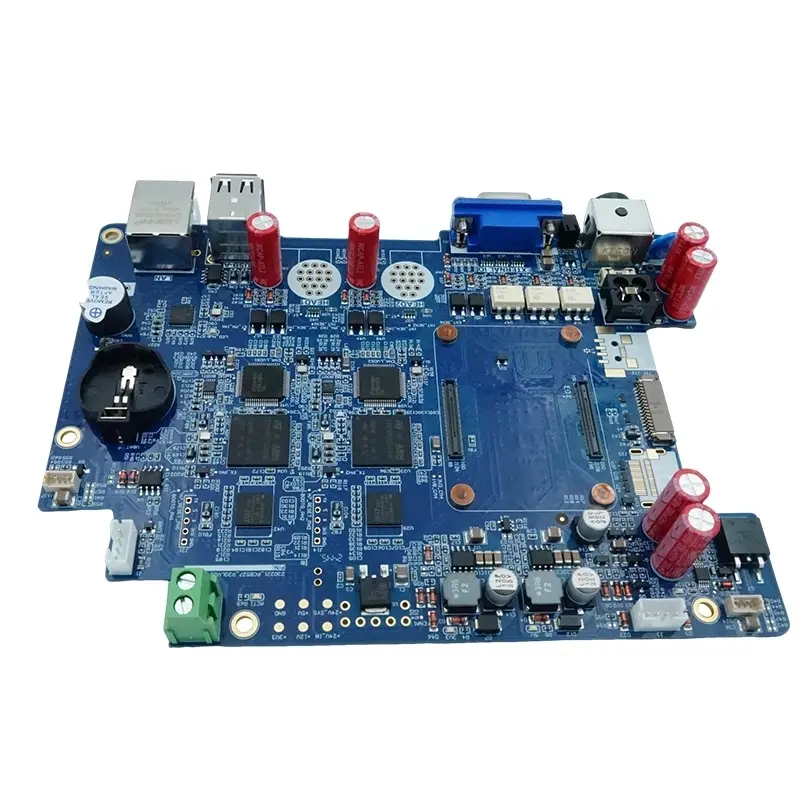
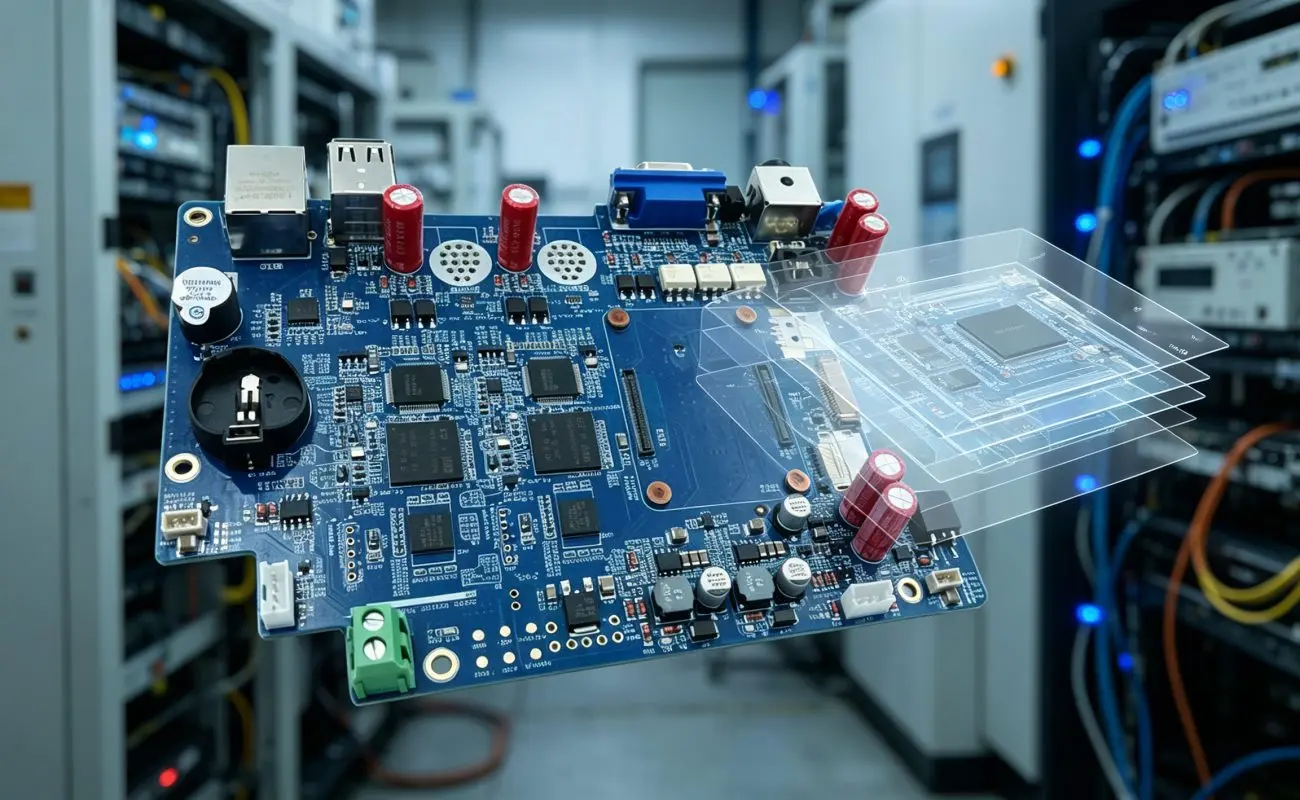
An 8-layer industrial communication PCB helps reduce signal interference through advanced layer structures, optimized routing designs, and precise manufacturing technologies. By separating signal and power layers, this PCB solution improves signal integrity while supporting high-speed communication interfaces such as Ethernet and CANopen.
Advanced Layer Structure Improves EMI Control
One of the main reasons signal interference occurs in communication systems is the interaction between high-speed signals and power circuits. Therefore, PCB layer design plays an important role in controlling electromagnetic interference. The 8-layer structure uses four signal layers and four power/ground planes, creating dedicated routing paths for different circuit functions. Moreover, the separated power and signal areas help reduce unwanted coupling between circuits. This design approach allows high-speed differential signals to travel through optimized paths with less noise impact. As a result, communication equipment can achieve more stable data transmission even in demanding industrial environments.
Precision Impedance Control Enhances Signal Integrity
High-speed communication requires accurate impedance management to prevent signal reflection and transmission errors. When impedance is inconsistent, signals may experience distortion, which can affect system reliability. The PCB supports controlled impedance design with differential line impedance maintained at 100Ω±8% and single-ended line impedance controlled at 50Ω±8%. Consequently, interfaces such as Gigabit Ethernet can maintain better signal quality during operation. Additionally, the 1OZ (35μm) copper thickness provides a balance between fine-line routing capability and current carrying performance. With a minimum line and space design of 75μm/75μm, the PCB supports complex circuit layouts while maintaining electrical stability.
Key Design Features For Reducing Signal Interference
The performance of communication PCBs depends on multiple design elements working together. Therefore, the following features contribute to improved signal protection and system reliability:
- 8-Layer Stackup Design: Separates signal and power layers to reduce electromagnetic coupling and improve routing efficiency.
- Controlled Impedance Technology: Minimizes signal reflection and supports stable high-speed communication.
- Optimized Ground Planes: Provides effective return paths for signals and helps suppress noise.
- 1OZ Copper Layers: Supports stable current transmission while maintaining precise circuit routing.
- ENIG Surface Finish: Improves connection reliability and protects conductive areas from oxidation.
- Mixed SMT And DIP Assembly: Combines high-density components with durable industrial connectors.
Fully Hong applies advanced PCB manufacturing technologies to help customers develop reliable communication boards for industrial applications. Through precise production control and optimized designs, these solutions support stable performance in complex operating environments.
Reliable Manufacturing Process For Industrial Applications
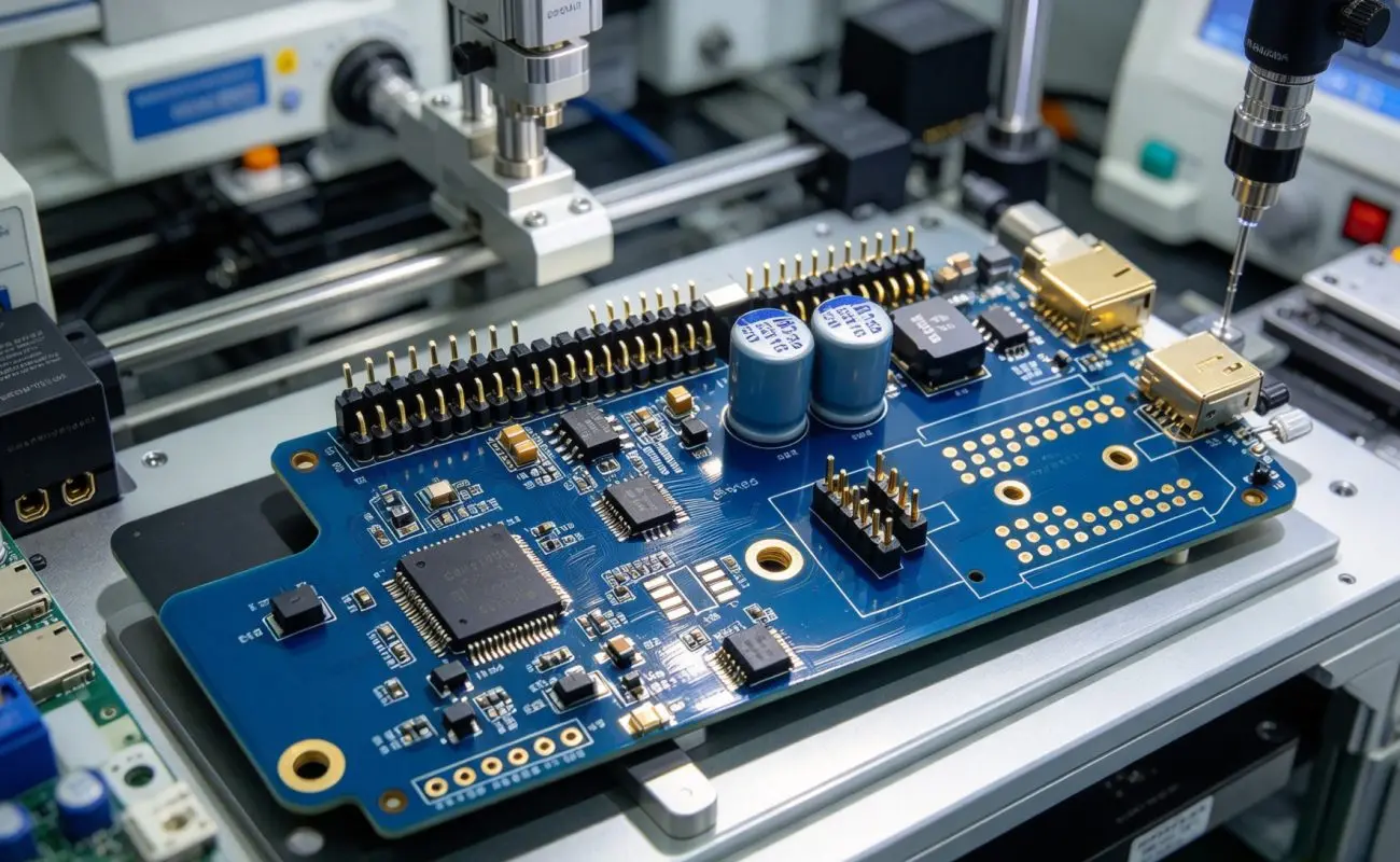
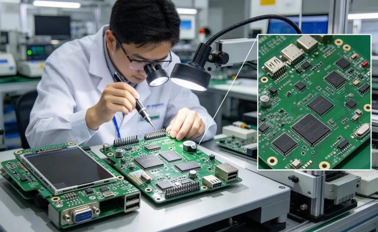
In addition to electrical design, manufacturing accuracy also affects the final communication performance. Therefore, advanced production technologies are necessary to maintain consistency and reliability. The PCB uses LDI (Laser Direct Imaging) technology to achieve high-precision trace production with 75μm accuracy. Furthermore, the electrolytic copper plating process maintains thickness uniformity within ±5%, helping ensure consistent electrical characteristics across the entire board.
The ENIG surface finish provides additional protection through a nickel layer of 4–6μm and a gold layer of 0.05–0.1μm. As a result, the board achieves improved corrosion resistance and long-term soldering reliability.
| Design Element | Contribution To Signal Stability |
|---|---|
| 8-Layer Stackup | Reduces EMI and improves signal routing efficiency |
| 100Ω Differential Impedance Control | Supports high-speed communication interfaces |
| 50Ω Single-Ended Impedance Control | Minimizes signal reflection problems |
| ENIG Surface Finish | Enhances connection durability and corrosion resistance |
| LDI Manufacturing Technology | Provides accurate circuit patterns and consistent performance |
Supporting Complex Industrial Communication Systems
Modern industrial communication equipment requires PCBs that can handle increasing data volumes while maintaining reliable connections. Therefore, advanced PCB designs are widely used in automation systems, industrial controllers, networking equipment, and smart manufacturing platforms.
The 8-layer industrial communication PCB provides a practical solution for applications that require strong signal integrity and stable communication performance. Its advanced stackup structure, precise impedance control, and durable manufacturing process allow it to operate effectively in environments with electromagnetic interference and continuous workloads. Moreover, the combination of SMT and DIP assembly compatibility enables flexible integration of different components, including PHY chips, FPGAs, RJ45 connectors, and industrial interfaces. This makes the PCB suitable for various communication hardware designs.
Conclusion
As industrial systems become more connected and intelligent, reducing signal interference has become a key challenge for PCB development. Through optimized layer structures, accurate impedance control, and advanced manufacturing methods, communication PCBs can provide more stable and efficient performance. Overall, the 8-layer industrial communication PCB offers an effective way to improve signal reliability, reduce electromagnetic interference, and support next-generation industrial communication systems. With professional manufacturing capabilities and customized design options, Fully Hong continues to provide dependable PCB solutions for modern industrial applications.



Leave a reply