2-layer FR4 TG170 PCB is engineered for applications requiring robust current handling and reliable performance in a cost-effective design, ideal for power supplies, LED drivers, and industrial control modules. Constructed from FR4 TG170 material (glass transition temperature 170°C), the PCB withstands high-temperature environments, making it suitable for components that generate significant heat. The 1.2mm thickness balances rigidity with weight, while the 2OZ (70μm) copper thickness on both layers supports high currents (up to 15A per trace), minimizing voltage drop and resistive heating.
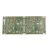
Designed in a 1×4 panel format, the PCB optimizes production efficiency for mass manufacturing, reducing material waste and lowering costs. Each panel contains four identical boards, streamlining assembly processes for high-volume orders. The Green LPI solder mask protects circuitry from moisture and chemical damage, while the White silkscreen provides clear component marking for easy assembly and maintenance. The ENIG (Electroless Nickel Immersion Gold) surface treatment ensures excellent solderability: the nickel layer (3–5μm) adds durability, and the gold layer (0.05–0.1μm) prevents oxidation, maintaining reliable connections over time.
A key feature is POFV (Plated Over Filled Vias) technology, where vias are filled with conductive material and plated to create a smooth, void-free surface. This eliminates the risk of solder wicking or thermal stress failure, critical for components subjected to repeated reflow cycles. POFV also enables via-in-pad designs, allowing tighter component spacing and more efficient routing in dense layouts.
Manufacturing processes prioritize precision and quality:
- DFM analysis optimizes panelization for minimal breakage during depaneling.
- Electrolytic copper plating ensures uniform 2OZ thickness, verified by cross-sectional tests.
- Laser drilling creates vias with ±10μm accuracy before POFV filling.
- 100% AOI inspection checks solder mask coverage and silkscreen clarity.
- Thermal stress testing confirms reliability at 260°C reflow temperatures.
Engineers will appreciate the PCB’s versatility in both power and signal applications. In consumer electronics, it suits chargers and adapters requiring high-current handling. In industrial settings, it excels in motor controls and power distribution blocks, where TG170 material ensures stability in warm environments. The 1×4 panel format is ideal for OEMs seeking economies of scale without compromising on performance.
By choosing this 2-layer FR4 TG170 PCB, customers gain a solution that merges 2OZ copper durability, POFV reliability, and panelized efficiency. Backed by IPC-6012 Class 2 compliance and RoHS certification, it delivers consistent quality from prototype to mass production—an optimal choice for cost-conscious projects that demand robust power handling and long-term reliability.

")