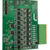
8-lớp PCB được thiết kế cho các ứng dụng truyền thông công nghiệp quan trọng, trong đó tính toàn vẹn của tín hiệu tần số cao, tương thích điện từ (EMC), và độ bền chắc chắn là rất cần thiết. Với kích thước của 190mm × 170mm và một 1.7độ dày mm, bo mạch cân bằng khả năng tích hợp thành phần quy mô lớn với độ ổn định cơ học cho tủ điều khiển công nghiệp và trung tâm truyền thông. Sự độc đáo Xếp chồng vật liệu TU-862+RO4350B kết hợp độ bền cơ học hiệu quả về mặt chi phí của TU-862 với đặc tính điện môi tổn thất thấp của RO4350B (Đk=3,48, tanδ=0,004 ở 10GHz), khiến nó trở nên lý tưởng cho việc truyền dữ liệu tốc độ cao trong các giao thức như Ethernet, CANopen, và PROFIBUS.
- Độ dày đồng không đối xứng:
- Lớp ngoài: 1Oz (35μm) cho dấu vết năng lượng mạnh mẽ và che chắn EMI
- Lớp bên trong: 0.5Oz (18μm) để định tuyến tín hiệu cao độ
- Cho phép phân phối điện năng cân bằng (4 Máy bay điện/mặt đất) và các lớp tín hiệu tốc độ cao (4 kênh cặp vi sai)
- Kiểm soát trở kháng chính xác:
- 50Ω ±8% đối với cấu hình microstrip/stripline
- Đạt được thông qua tính toán độ dày điện môi và chiều rộng vết được kiểm soát
- Giảm thiểu phản xạ tín hiệu trong Ethernet 10Gbps và giao diện không dây công nghiệp
- Vias đầy không dẫn điện (NCFV) với nắp đồng:
- Vias chứa đầy nhựa để ngăn chặn khoảng trống, sau đó phủ đồng để hoàn thiện bề mặt mịn
- Loại bỏ rủi ro thấm hút hàn ở khu vực BGA và cải thiện độ dẫn nhiệt
- Cán tuần tự:
- 8 các lớp được ép theo từng giai đoạn để đảm bảo độ dày điện môi đồng đều và độ chính xác đăng ký (<50μm)
- Bề mặt hoàn thiện ENIG:
- 3-5Lớp niken μm để chống ăn mòn
- 0.05-0.1Lớp vàng μm cho khả năng hàn lâu dài
- Mặt nạ hàn LPI xanh Matt:
- Giảm độ chói trong quá trình kiểm tra AOI
- Cung cấp khả năng kháng hóa chất vượt trội trong môi trường công nghiệp
- Giảm thiểu EMC/EMI:
- Các lỗ khâu trên mặt đất được đặt cách nhau 2 mm để triệt tiêu tiếng ồn ở chế độ chung
- Định tuyến cặp vi sai chính xác với độ dài phù hợp được kiểm soát bên trong 5 Mils (0.127mm) để đảm bảo độ lệch tín hiệu tối thiểu
- Quản lý nhiệt:
- Vias nhiệt kết nối các mặt phẳng điện với các lớp bên ngoài để tản nhiệt hiệu quả
- Khu vực đổ đồng trên các lớp năng lượng để giảm các điểm nóng
- Hỗ trợ lắp ráp hỗn hợp:
- SMT cho IC mật độ cao (ví dụ., chip PHY, FPGA)
- DIP cho đầu nối chắc chắn (ví dụ., RJ45, DB25) và rơle
- 100% Kiểm tra tự động:
- Xác minh trở kháng trên mỗi lớp
- Kiểm tra bằng tia X của NCFV vias
- AOI cho mặt nạ hàn và chất lượng lụa
- Kiểm tra môi trường:
- Chu kỳ nhiệt độ (-40° C đến +85 ° C., 1,000 chu kỳ)
- Kiểm tra rung động (5-500Hz, 2G Tăng tốc)
- Tuân thủ tiêu chuẩn:
- Lớp IPC-6012 3 cho các ứng dụng quan trọng
- RoHS/REACH để hạn chế chất độc hại
- TRONG 55032 Loại A cho phát xạ điện từ
- Bộ chuyển mạch Ethernet công nghiệp:
Hỗ trợ 10GBASE-T và PoE+ với mức suy giảm tín hiệu tối thiểu
- Trạm cơ sở không dây:
Cho phép định tuyến tần số vô tuyến dưới 6GHz 5G NR
- PLC & Hệ thống SCADA:
Tạo điều kiện trao đổi dữ liệu theo thời gian thực trong các nhà máy sản xuất
- Mạng thông tin liên lạc đường sắt:
Gặp nhau 50155 Tiêu chuẩn môi trường đối với ứng dụng đầu máy toa xe

")