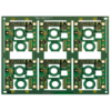
8-lớp FR4 PCB được thiết kế cho các thiết kế điện tử mật độ cao đòi hỏi sự cân bằng về tính toàn vẹn tín hiệu, Phân phối điện, và các yếu tố hình thức nhỏ gọn, như điện tử tiêu dùng, thiết bị y tế, và mô-đun điều khiển công nghiệp. Các 8-Kiến trúc lớp (tiêu biểu 4 Lớp tín hiệu + 4 Máy bay điện/mặt đất) cho phép định tuyến phức tạp cho các thành phần có bước cao đồng thời giảm thiểu nhiễu điện từ (Emi). Các 1.2Độ dày mm cung cấp một nền tảng nhẹ nhưng cứng nhắc, lý tưởng cho các ứng dụng có không gian hạn chế, nơi trọng lượng và độ bền là rất quan trọng.
Được xây dựng với vật liệu FR4, PCB cung cấp cách điện đáng tin cậy (Hằng số điện môi εr = 4,5) và độ ổn định cơ học, thích hợp cho nhiều môi trường hoạt động. Các 2Oz (70μm) Độ dày đồng trên tất cả các lớp tăng cường khả năng mang dòng điện (lên đến 15a mỗi dấu vết) trong khi vẫn duy trì tính linh hoạt trong thiết kế cho cả dấu vết nguồn và tín hiệu. Các LPI xanh (Có thể chụp được chất lỏng) mặt nạ hàn không chỉ bảo vệ mạch khỏi tác hại của môi trường mà còn cải thiện độ chính xác của việc kiểm tra trực quan, Trong khi Silkscreen trắng đảm bảo đánh dấu và chỉ định thành phần rõ ràng để lắp ráp và bảo trì.
Một tính năng quan trọng là Đồng ý (Điện phân Niken Vàng) xử lý bề mặt, mang lại sự mượt mà, kết thúc chống ăn mòn cho khả năng hàn tuyệt vời. Lớp niken (3Mạnh5μm) Thêm độ bền, và lớp vàng (0.05Cấm0,1mm) ngăn chặn quá trình oxy hóa, làm cho nó phù hợp để sử dụng lâu dài. Các POFV (Mạ trên Vias đầy) công nghệ nâng cao hơn nữa độ tin cậy của PCB: vias được lấp đầy bằng vật liệu dẫn điện và được mạ lên trên, loại bỏ các khoảng trống có thể gây ra ứng suất nhiệt hoặc thấm hút hàn. Điều này đặc biệt quan trọng đối với các thiết kế có mật độ cao với các thành phần bước cao (ví dụ., 0.5mm sân BGA) và đảm bảo hiệu suất ổn định trong quá trình hàn nóng chảy lại.
Việc sản xuất PCB này liên quan đến các kỹ thuật tiên tiến để đảm bảo độ chính xác và chất lượng:
- Hình ảnh trực tiếp bằng laser (LDI) đạt được độ chính xác đường nét (Chiều rộng/không gian dòng tối thiểu: 50µm/50µm) để định tuyến phức tạp.
- xử lý POFV sử dụng epoxy hoặc nhựa dẫn điện để lấp đầy vias, tiếp theo là mạ để tạo bề mặt nhẵn.
- 100% Aoi (Kiểm tra quang học tự động) xác minh độ che phủ của mặt nạ hàn và độ trong của màn lụa.
- Thử nghiệm điện đảm bảo tính liên tục và khả năng chống cách ly, Gặp gỡ lớp IPC-6012 2 tiêu chuẩn.
Các kỹ sư sẽ đánh giá cao tính linh hoạt của PCB trong việc xử lý cả định tuyến tín hiệu mật độ cao và ứng dụng năng lượng vừa phải. Trong điện tử tiêu dùng, nó hỗ trợ các thiết kế nhỏ gọn cho điện thoại thông minh, máy tính bảng, và thiết bị đeo, nơi không gian được đánh giá cao. Trong thiết bị y tế, Công nghệ POFV và lớp hoàn thiện ENIG góp phần mang lại độ tin cậy lâu dài cho thiết bị chẩn đoán. Trong hệ thống công nghiệp, vật liệu đồng 2OZ và FR4 mang lại độ bền cần thiết cho bảng điều khiển và mô-đun tự động hóa.
Bằng cách chọn PCB FR4 8 lớp với đồng 2OZ này, kết thúc ENIG, và công nghệ POFV, khách hàng có được giải pháp cân bằng mật độ, độ tin cậy, và hiệu quả chi phí. Sự kết hợp tiên tiến của nó thông qua việc làm đầy, xử lý bề mặt cao cấp, và khả năng sản xuất chính xác khiến nó trở thành lựa chọn chiến lược cho các ứng dụng cần tích hợp thành phần và hiệu suất lâu dài. Được hỗ trợ bởi ISO 9001:2015 chứng nhận, PCB này đảm bảo chất lượng nhất quán từ tạo mẫu đến sản xuất hàng loạt.

")