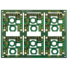
8-FR4 katmanı PCB, sinyal bütünlüğünde denge gerektiren yüksek yoğunluklu elektronik tasarımlar için tasarlanmıştır, güç dağıtımı, ve kompakt form faktörleri, tüketici elektroniği gibi, tıbbi cihazlar, ve endüstriyel kontrol modülleri. . 8-katman mimarisi (tipik olarak 4 sinyal katmanları + 4 Güç/Zemin Uçakları) Elektromanyetik paraziti en aza indirirken ince aralıklı bileşenler için karmaşık yönlendirmeye olanak tanır (EMI). . 1.2MM tahta kalınlığı hafif ancak sağlam bir temel sunar, ağırlık ve dayanıklılığın kritik olduğu, alanın kısıtlı olduğu uygulamalar için idealdir.
İle inşa edilmiş FR4 malzemesi, PCB güvenilir elektrik yalıtımı sağlar (Dielektrik sabiti εr = 4.5) ve mekanik stabilite, çok çeşitli çalışma ortamlarına uygun. . 2Oz (70μm) bakır kalınlığı tüm katmanlarda akım taşıma kapasitesini artırır (İz başına 15a'ya kadar) hem güç hem de sinyal izleri için tasarım esnekliğini korurken. . Yeşil LPI (Sıvı Fotoğrafla Görüntülenebilir) lehim maskesi Devreyi yalnızca çevresel hasarlardan korumakla kalmaz, aynı zamanda görsel denetim doğruluğunu da artırır, iken Beyaz ipek montaj ve bakım için net bileşen işaretlemesi ve tanımlamaları sağlar.
Önemli bir özellik, Kabul etmek (Elektroles Nikel Daldırma Altın) yüzey işleme, pürüzsüz bir ortam sağlar, Mükemmel lehimlenebilirlik için korozyona dayanıklı kaplama. Nikel tabakası (3–5μm) dayanıklılık ekler, Ve altın katman (0.05–0.1mm) oksidasyonu önler, uzun süreli kullanıma uygun hale getirir. . POFV (Kaplamalı Üzeri Doldurulmuş Vialar) teknolojisi PCB'nin güvenilirliğini daha da artırır: vialar iletken malzeme ile doldurulur ve üzeri kaplanır, termal strese veya lehim fitillenmesine neden olabilecek boşlukları ortadan kaldırır. Bu, özellikle ince adımlı bileşenlere sahip yüksek yoğunluklu tasarımlar için önemlidir. (Örn., 0.5mm aralıklı BGA'lar) ve yeniden akışlı lehimleme işlemlerinde tutarlı performans sağlar.
Bu PCB'nin üretimi, hassasiyet ve kalite sağlamak için gelişmiş teknikler içerir.:
- Lazer Doğrudan Görüntüleme (LDI) ince çizgi doğruluğuna ulaşır (Minimum çizgi genişliği/boşluk: 50µm/50μm) karmaşık yönlendirme için.
- POFV işleme viaları doldurmak için iletken epoksi veya reçine kullanır, ardından pürüzsüz bir yüzey oluşturmak için kaplama yapılır.
- 100% AOI (Otomatik Optik İnceleme) lehim maskesi kapsamını ve serigrafi netliğini doğrular.
- Elektrik Testi süreklilik ve izolasyon direnci sağlar, Buluşma IPC-6012 Sınıfı 2 standartlar.
Mühendisler, PCB'nin hem yüksek yoğunluklu sinyal yönlendirmeyi hem de orta düzey güç uygulamalarını yönetmedeki çok yönlülüğünü takdir edeceklerdir. Tüketici elektroniğinde, akıllı telefonlar için kompakt tasarımları destekler, tabletler, ve giyilebilir cihazlar, alanın öncelikli olduğu yer. Tıbbi cihazlarda, POFV teknolojisi ve ENIG kaplaması teşhis ekipmanlarında uzun vadeli güvenilirliğe katkıda bulunur. Endüstriyel sistemlerde, 2OZ bakır ve FR4 malzemesi kontrol panelleri ve otomasyon modülleri için gereken dayanıklılığı sağlar.
2OZ bakırlı bu 8 katmanlı FR4 PCB'yi seçerek, ENIG bitişi, ve POFV teknolojisi, müşteriler yoğunluğu dengeleyen bir çözüm elde ediyor, güvenilirlik, ve maliyet etkinliği. Doldurma yoluyla gelişmiş kombinasyonu, birinci sınıf yüzey işlemi, ve hassas üretim, bileşen entegrasyonunun ve uzun vadeli performansın önemli olduğu uygulamalar için onu stratejik bir seçim haline getiriyor. ISO tarafından desteklendi 9001:2015 sertifikasyon, Bu PCB prototiplemeden seri üretime kadar tutarlı kalite sağlar.

")