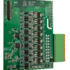
8-Слойная печатная плата разработана для критически важных приложений промышленной связи., где целостность высокочастотного сигнала, электромагнитная совместимость (EMC), и надежная долговечность имеют важное значение. С размерами 190мм×170 мм и 1.7ММ толщина, Плата сочетает в себе крупномасштабную интеграцию компонентов с механической стабильностью для промышленных шкафов управления и узлов связи.. Уникальный Сборка материалов ТУ-862+РО4350Б сочетает в себе экономичную механическую прочность TU-862 с диэлектрическими свойствами RO4350B с низкими потерями. (Дк=3,48, tanδ=0,004 на частоте 10 ГГц), что делает его идеальным для высокоскоростной передачи данных по таким протоколам, как Ethernet., Канопен, и ПРОФИБУС.
- Асимметричная толщина меди:
- Внешние слои: 1Унция (35мкм) для надежных силовых линий и защиты от электромагнитных помех
- Внутренние слои: 0.5Унция (18мкм) для тонкой маршрутизации сигналов
- Обеспечивает сбалансированное распределение мощности (4 Силовая/основные плоскости) и высокоскоростные сигнальные слои (4 каналы дифференциальной пары)
- Прецизионный контроль импеданса:
- 50Ом ±8% для микрополосковых/полосковых конфигураций
- Достигается путем контролируемых расчетов толщины диэлектрика и ширины дорожки.
- Минимизирует отражение сигнала в Ethernet 10 Гбит/с и промышленных беспроводных интерфейсах.
- Непроводящие заполненные переходные отверстия (НЦФВ) с медным покрытием:
- Переходные отверстия заполнены смолой для предотвращения пустот., затем покрыт медью для гладкой поверхности
- Устраняет риск затекания припоя в области BGA и улучшает теплопроводность.
- Последовательное ламинирование:
- 8 слои ламинируются поэтапно, чтобы обеспечить равномерную толщину диэлектрика и точность регистрации. (<50мкм)
- Загадочная поверхность отделка:
- 3-5Слой никеля мкм для устойчивости к коррозии
- 0.05-0.1Слой золота мкм для длительной пайки
- Матово-зеленая паяльная маска LPI:
- Уменьшает блики во время проверки AOI
- Обеспечивает превосходную химическую стойкость в промышленных средах.
- Смягчение электромагнитной совместимости и электромагнитных помех:
- Сшивающие сквозные отверстия наземной плоскости расположены с интервалом 2 мм для подавления синфазного шума.
- Прецизионная прокладка дифференциальных пар с точным контролем соответствия длины 5 мил (0.127мм) для обеспечения минимального перекоса сигнала
- Тепловое управление:
- Тепловые переходы, соединяющие силовые плоскости с внешними слоями для эффективного рассеивания тепла.
- Области заливки меди на силовых слоях для уменьшения количества горячих точек
- Поддержка смешанной сборки:
- SMT для микросхем высокой плотности (НАПРИМЕР., PHY-чипы, ПЛИС)
- DIP для прочных разъемов (НАПРИМЕР., RJ45, ДБ25) и реле
- 100% Автоматизированное тестирование:
- Проверка импеданса для каждого слоя
- Рентгеновский контроль переходных отверстий NCFV
- AOI для паяльной маски и качества шелкографии
- Экологические испытания:
- Температурный цикл (-40° C до +85 ° C., 1,000 цикл)
- Вибрационное тестирование (5-500Гц, 2G ускорение)
- Соответствие стандартам:
- IPC-6012 Класс 3 Для критически важных применений
- RoHS/REACH для ограничений по опасным веществам
- В 55032 Класс А по электромагнитному излучению
- Промышленные Ethernet-коммутаторы:
Поддерживает 10GBASE-T и PoE+ с минимальным ухудшением сигнала.
- Беспроводные базовые станции:
Обеспечивает маршрутизацию радиочастот 5G NR ниже 6 ГГц.
- ПЛК & Scada Systems:
Облегчает обмен данными в режиме реального времени на производственных предприятиях.
- Сети железнодорожной связи:
Встречается в 50155 экологические стандарты для применения подвижного состава

")